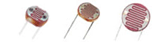
Token Electronics now offers commercial grade PGM photoresistor. Designated the PGM Series, the photoresistors are available in 5mm, 12mm and 20mm sizes, the conformally epoxy or hermetical package offer high quality performance for applications that require quick response and good characteristic of spectrum.
Visible light sensors are used to detect light or illumination using a manner similar to the human eye. They are typically used in industrial lighting, consumer electronics, and vehicle systems, where they allow settings to be adjusted automatically in response to changing ambient light conditions.
A phototransistor is known as a device in which turns light source energy into electric energy. Phototransistors are very close to photoresistors but produce both current and voltage, while photoresistors simply produce current. The reason is a phototransistor includes a bipolar semiconductor and targets the energy this can be transmitted via it.
Ambient light sensors (ALS) will also be known as illuminance or illumination sensors, photodetector, brightness sensors, photo transistor, optical sensors, or simply light sensors. One essential application for ALS technologies are mobile phones. Inside a mobile phone, the ALS enables automatic charge of display backlight brightness over an array of illumination conditions from the dark atmosphere to sunlight.
Maximum value of limit per each item.
Allowable temperature range of power application. Usually when the operating temperature increases, the power consumption decreases.
In addition, the power application is prohibited when the actual operating temperature is out of range.
In the case of a phototransistor, the temperature that can be applied is not described as the surface temperature of the package, but is described as working temperature (the ambient air temperature around the device).
In the stored state, allowable temperature range when power is not applied.
When the operating temperature is 25°C, the light receives the allowable power dissipation of the phototransistor. Often, as the ambient temperature increases, the allowable power consumption (PC) tends to drop.
When the light-receiving phototransistor conducts current at 25°C ambient temperature, the maximum allowable collector current flows through the phototransistor in the permissible power dissipation (PC) range.
λp Is the most sensitive wavelength value of the phototransistor, measured in nanometers (nm).
The Phototransistor responds to the light from the wavelength range of the fluorescence or incandescent light source, and when matched with the IR LED light source, they perform optimally. This is because the phototransistor has a peak spectral response at approximately 840nm of near-infrared.
VBR is the maximum voltage allowed between the collector and emitter. Exceeding the maximum voltage can cause permanent damage to the phototransistor. The breakdown voltages are 100% sorting parameters.
The maximum voltage is allowed between the collector and the emitter on light-receiving side, and when no forward current flows through the led of the light emission side (the indicator light does not emit light).
Under normal circumstances, when the power supply voltage close to this value, the transient operating trajectory can not be maintained at the actual maximum operating temperature of the allowable power range, in the process of switching, the device may occur over power damage.
Note that the supply voltage is kept within a sufficient safe range so that no excessive power loss occurs even during this switching moment.
The infrared phototransistor acts as a transistor, and its basic voltage is determined by the amount of light that impinges on the transistor.
Therefore, it acts as a variable current source. More IR light will cause a larger current to flow through the collector-emitter lead. IL(4) is specified at VEC = 5V, IR LED 850nm.
The allowable reverse voltage of the phototransistor that can be applied to the light receiving side.
Typically, the voltage depends on the reverse withstand voltage between the emitter and the base of the phototransistor, or below the reverse withstand voltage. Damage or irreversible damage may occur if a reverse voltage exceeding this value is applied.
When the phototransistor is in the dark and a voltage is applied from the collector to the emitter, a certain amount of current will flow.
This current is called a dark current. The current consists of the collector-base junction leakage current and the transistor's DC current gain.
The presence of this current prevents the phototransistor from being considered "off", or is ideal for "on" the switch. The dark current is specified as the maximum collector current that allows flow at a given collector-emitter test voltage.
The dark current is a function of the applied collector-emitter voltage and ambient temperature. Dark current increases with increasing temperature.
This value is usually pecified at 25°C. The value of the load resistance must be designed with the maximum value of the current within the conditions of use.
Saturation is the state in which both the emitter base and the collector base of the phototransistor become forward based.
From a practical point of view, the collector-emitter saturation voltage Vce(sat) is a factor that represents the proximity switch (closed state) of the photodetector.
This is because Vce(sat) is the voltage that drops when the detector is in the "on" state.
Vce(sat) is usually the maximum allowable collector emitter voltage given the specified light intensity and collector current value.
| Parameter | Symbol | Condition | Min. | Typ. | Max. | Unit |
| Photo Current | IL(1) | Vcc=5V Ev=10Lux |
1.2 | 2.5 | 3.6 | μA |
| IL(2) | Vcc=5V Ev=30Lux |
3.6 | 7.5 | 10.8 | μA | |
| IL(3) | Vcc=5V Ev=100Lux |
12 | 25 | 36 | μA | |
| Collector Dark Current | ID | Vcc=5V/85°C Ev=0Lux |
- | - | 0.8 | μA |
| Batch BINNED GROUP (Tamb = 25 °C, unless otherwise specified) | ||||||
| Parameter | Condition | Binned Group | Symbol | Min. | Max. | Unit |
| Photo Current | EV = 100 lux, CIE illuminant A, VCE = 5 V | A | IPCE | 12 | 23 | μA |
| B | IPCE | 19 | 36 | μA | ||
Token provides ambient light sensor for photodiode and phototransistor. For a given irradiance, the phototransistor may show a batch change of the output current due to the susceptibility of the wafer and the variability of the transistor gain.
The lot-to-lot change of the photoelectric sensor is significantly lower because it is only caused by the variability of photosensitivity. Token provides phototransistor output (component) for its ambient light sensor in binned groups (Table 2).
These groups can not be ordered separately, but each reel is labeled A, B, or C, which allows the user to select the appropriate load resistance to compensate for these wide tolerances.
In order to minimize the output variability of the light sensor, the load resistance (RL) requires the selection of the component to choose the load resistance (RL) according to the sorted standard illuminance.
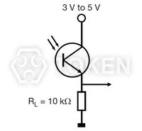
The ambient light sensor and the transistor output of the typical optical circuit shown in Figure 3. For the PT-IC-GC-3-PE-520, 30 lux the typical output current is 7.5 μA. At 100 lux, the typical output current is 25 μA and the output current is in the range of 12 μA to 36μA.
By the previously mentioned binning components, the range of 100 lux is divided into two bins. Each bin should use a different load resistor, and the output is relatively consistent for a given lux level.
Suppose application detection ranges from 10 lux to $1000 lux. Use a 10 KΩ load resistor to produce a voltage of 0.025 V to 2.5 V. The photocurrent of the voltage is equal to 2.5 μA to 250 μA.
| Part Number | Bin | Photocurrent, IPCE at 100 lux (μA) | ||
| Min. | Mean | Max. | ||
| PT-IC-GC-3-PE-520 | A | 12 | 17.5 | 23 |
| B | 19 | 27.5 | 36 | |
| Bin A | Bin B |
| IPCE = 17.5 μA, RL = 10 kΩ V = 17.5 μA x 10 kΩ V = 175 mV |
0.175 V = 0.0000275 A x RL R L = 0.175 V/0.0000275 A R L = 6.36 kΩ |
Download Select The Load Resistor in PDF file.
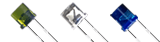
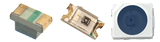
| Category | Thumb Nail | Part NO. | Infrared Ray | Lens Color | Spectral Bandwidth (nm) |
Photo Current | Dark Current | ||
| 10Lux | 30Lux | 100Lux | 0Lux | ||||||
| Φ3 Plate Edge | PT-A6-BC-3-PE-520 | IR Receiving | Dark Blue | 520 | 3 ~ 12 | 9 ~ 36 | 30 ~ 120 | 0.2Max. | |
| PT-IC-BC-3-PE-550 | IR Receiving | Dark Blue | 550 | 1.5 ~ 5.0 | 4.5 ~ 15 | 15 ~ 50 | 0.8Max. | ||
| PT-IC-GC-3-PE-520 | IR Receiving | Dark Green | 520 | 1.2 ~ 3.6 | 3.6 ~ 10.8 | 12 ~ 36 | 0.8Max. | ||
| PT-IC-AC-3-PE-550 | IR Receiving | Water Clear | 550 | 7 ~ 15 | 21 ~ 54 | 70 ~ 180 | 0.8Max. | ||
| PT-A1-AC-3-PE-850 | IR Blocking | Water Clear | 850 | 3 ~ 6 | 9 ~ 18 | 30 ~ 60 | 0.1Max. | ||
| Φ5 Plate Edge | PT-IC-GC-5-PE-520 | IR Receiving | Dark Green | 520 | 2 ~ 6 | 6 ~ 18 | 20 ~ 60 | 0.8Max. | |
| PT-IC-BC-5-PE-550 | IR Receiving | Dark Blue | 550 | 2.5 ~ 5.5 | 7.5 ~ 16.5 | 25 ~ 55 | 0.8Max. | ||
| PT-IC-AC-5-PE-550 | IR Receiving | Water Clear | 550 | 7 ~ 18 | 21 ~ 54 | 70 ~ 180 | 0.8Max. | ||
| PT-A2-AC-5-PE-850 | IR Blocking | Water Clear | 850 | 1.5 ~ 4.5 | 4.5 ~ 13.5 | 15 ~ 45 | 0.1Max. | ||
| Φ5 Helmet Edge | PT-A1-AC-5-HE-850 | IR Blocking | Water Clear | 850 | 4.5 ~ 9.0 | 13.5 ~ 27 | 45 ~ 90 | 0.1Max. | |
| Φ5 Plate None | PT-A6-AC-5-PN-580 | IR Receiving | Water Clear | 580 | 2.5 ~ 10 | 7.5 ~ 30 | 25 ~ 100 | 0.2Max. | |
| PT-IC-BC-5-PN-550 | IR Receiving | Dark Blue | 550 | 2.5 ~ 5.5 | 7.5 ~ 16.5 | 25 ~ 55 | 0.8Max. | ||
| PT-IC-AC-5-PN-580 | IR Receiving | Water Clear | 580 | 1.5 ~ 5.5 | 4.5 ~ 16.5 | 15 ~ 55 | 0.8Max. | ||
| PT-A4-AC-5-PN-850 | IR Blocking | Water Clear | 850 | 5 ~ 12 | 15 ~ 36 | 50 ~ 120 | 0.1Max. | ||
| PT-A2-AC-5-PN-850 | IR Blocking | Water Clear | 850 | 1.5 ~ 4.5 | 4.5 ~ 13.5 | 15 ~ 45 | 0.1Max. | ||
| Φ3 Bullet Edge | PT-A2-AC-3-BE-850 | IR Blocking | Water Clear | 850 | 15 ~ 45 | 45 ~ 145 | 150 ~ 450 | 0.1Max. | |
| PT-A2-DC-3-BE-940 | IR Blocking | Dark | 940 | - | - | - | 0.1Max. | ||
| Φ5 Bullet Edge | PT-A2-AC-5-BE-850 | IR Blocking | Water Clear | 850 | 30 ~ 90 | 90 ~ 270 | 300 ~ 900 | 0.1Max. | |
| PT-A1-FC-5-BE-940 | IR Blocking | Dark | 940 | - | - | - | 0.1Max. | ||
| Φ5 Bullet None | PT-A6-AC-5-BN-520 | IR Receiving | Water Clear | 520 | 5 ~ 22 | 15 ~ 66 | 50 ~ 220 | 0.2Max. | |
| PT-IC-AC-5-BN-520 | IR Receiving | Water Clear | 520 | 4 ~ 12 | 12 ~ 36 | 40 ~ 120 | 0.8Max. | ||
| PT-A1-DC-5-BN-940 | IR Blocking | Dark | 940 | - | - | - | 0.1Max. | ||
| SMD | PT-B1-DC-0603-940 | IR Receiving | Dark | 940 | - | - | - | 0.1Max. | |
| PT-A8-AC-1206-850 | IR Receiving | Water Clear | 850 | 0.5 ~ 1.2 | 1.5 ~ 3.6 | 5 ~ 12 | 0.1Max. | ||
| PT-IC-BC-3528-550 | IR Blocking | Dark Blue | 550 | 1.5 ~ 4.5 | 4.5 ~ 13.5 | 15 ~ 45 | 0.1Max. | ||
| PT-IC-AC-3528-520 | IR Blocking | Water Clear | 520 | 7 ~ 18 | 21 ~ 54 | 70 ~ 180 | 0.8Max. | ||
| PT-A1-AC-3528-850 | IR Blocking | Water Clear | 850 | 2.5 ~ 5.0 | 7.5 ~ 15 | 25 ~ 50 | 0.1Max. | ||
| CdS (PGM5) |  |
PGM5506 | IR Blocking | Epoxy Resin | 540 | 2 ~ 6 | - | - | 0.15Min. |
| PGM5516 | IR Blocking | Epoxy Resin | 540 | 5 ~ 10 | - | - | 0.2Min. | ||
| PGM5526 | IR Blocking | Epoxy Resin | 540 | 8 ~ 20 | - | - | 1.0Min. | ||
| PGM5537 | IR Blocking | Epoxy Resin | 540 | 16 ~ 50 | - | - | 2.0Min. | ||
| PGM5539 | IR Blocking | Epoxy Resin | 540 | 30 ~ 90 | - | - | 5.0Min. | ||
| PGM5549 | IR Blocking | Epoxy Resin | 540 | 45 ~ 140 | - | - | 10.0Min. | ||
| PGM5616D | IR Blocking | Epoxy Resin | 560 | 5 ~ 10 | - | - | 1.0Min. | ||
| PGM5626D | IR Blocking | Epoxy Resin | 560 | 8 ~ 20 | - | - | 2.0Min. | ||
| PGM5637D | IR Blocking | Epoxy Resin | 560 | 16 ~ 50 | - | - | 5.0Min. | ||
| PGM5639D | IR Blocking | Epoxy Resin | 560 | 30 ~ 90 | - | - | 10.0Min. | ||
| PGM5649D | IR Blocking | Epoxy Resin | 560 | 50 ~ 160 | - | - | 20.0Min. | ||
| PGM5659D | IR Blocking | Epoxy Resin | 560 | 150 ~ 300 | - | - | 20.0Min. | ||
 |
PGM5506-MP | IR Blocking | Hermetical | 540 | 2 ~ 6 | - | - | 0.15Min. | |
| PGM5516-MP | IR Blocking | Hermetical | 540 | 5 ~ 10 | - | - | 0.2Min. | ||
| PGM5526-MP | IR Blocking | Hermetical | 540 | 8 ~ 20 | - | - | 1.0Min. | ||
| PGM5537-MP | IR Blocking | Hermetical | 540 | 16 ~ 50 | - | - | 2.0Min. | ||
| PGM5539-MP | IR Blocking | Hermetical | 540 | 30 ~ 90 | - | - | 5.0Min. | ||
| PGM5549-MP | IR Blocking | Hermetical | 540 | 45 ~ 140 | - | - | 10.0Min. | ||
| CdS (PGM12) |  |
PGM1200 | IR Blocking | Epoxy Resin | 560 | 2 ~ 5 | - | - | 1.0Min. |
| PGM1201 | IR Blocking | Epoxy Resin | 560 | 4 ~ 10 | - | - | 2.0Min. | ||
| PGM1202 | IR Blocking | Epoxy Resin | 560 | 8 ~ 20 | - | - | 5.0Min. | ||
| PGM1203 | IR Blocking | Epoxy Resin | 560 | 18 ~ 50 | - | - | 10.0Min. | ||
| PGM1204 | IR Blocking | Epoxy Resin | 560 | 45 ~ 150 | - | - | 20.0Min. | ||
| PGM1205 | IR Blocking | Epoxy Resin | 560 | 140 ~ 300 | - | - | 20.0Min. | ||
 |
PGM1200-MP | IR Blocking | Hermetical | 560 | 2 ~ 5 | - | - | 1.0Min. | |
| PGM1201-MP | IR Blocking | Hermetical | 560 | 4 ~ 10 | - | - | 2.0Min. | ||
| PGM1202-MP | IR Blocking | Hermetical | 560 | 8 ~ 20 | - | - | 5.0Min. | ||
| PGM1203-MP | IR Blocking | Hermetical | 560 | 18 ~ 50 | - | - | 10.0Min. | ||
| PGM1204-MP | IR Blocking | Hermetical | 560 | 45 ~ 150 | - | - | 20.0Min. | ||
| PGM1205-MP | IR Blocking | Hermetical | 560 | 140 ~ 300 | - | - | 20.0Min. | ||
| CdS (PGM20) |  |
PGM2000 | IR Blocking | Epoxy Resin | 560 | 2 ~ 5 | - | - | 1.0Min. |
| PGM2001 | IR Blocking | Epoxy Resin | 560 | 4 ~ 10 | - | - | 2.0Min. | ||
| PGM2002 | IR Blocking | Epoxy Resin | 560 | 8 ~ 20 | - | - | 5.0Min. | ||
| PGM2003 | IR Blocking | Epoxy Resin | 560 | 18 ~ 50 | - | - | 10.0Min. | ||
| PGM2004 | IR Blocking | Epoxy Resin | 560 | 45 ~ 150 | - | - | 20.0Min. | ||
| PGM2005 | IR Blocking | Epoxy Resin | 560 | 140 ~ 300 | - | - | 20.0Min. | ||
 |
PGM2000-PP | IR Blocking | Plactic Case | 560 | 2 ~ 5 | - | - | 1.0Min. | |
| PGM2001-PP | IR Blocking | Plactic Case | 560 | 4 ~ 10 | - | - | 2.0Min. | ||
| PGM2002-PP | IR Blocking | Plactic Case | 560 | 8 ~ 20 | - | - | 5.0Min. | ||
| PGM2003-PP | IR Blocking | Plactic Case | 560 | 18 ~ 50 | - | - | 10.0Min. | ||
| PGM2004-PP | IR Blocking | Plactic Case | 560 | 45 ~ 150 | - | - | 20.0Min. | ||
| PGM2005-PP | IR Blocking | Plactic Case | 560 | 140 ~ 300 | - | - | 20.0Min. | ||
| Ambient Light Sensors | Light Dependent Resistor (LDR) Photoresistor (CdS) |
 |
Advantages: similar to the human eye. Disadvantages: Cadmium, ROHS prohibited substances. |
| Photodiode |  |
Advantages: The uniformity of the photodiode between the units is relatively high. Disadvantages: low current output, the need for external amplification circuit. |
|
| Phototransistor Photosensitive Sensor Photosensitive Triode |
Advantages: with amplifier circuit, photoelectric transistor output current. Disadvantages: poor temperature characteristics. |
||
| Photo IC | Advantages: amplification, logic control, switches and other integrated features Disadvantages: high dependence on professional products. |
The environmentally friendly phototransistor is a combination of photodiode and amplifier integrated in a single chip. This integrated combination is used to overcome the main uniform gain limits of the photodiode.
Many modern applications require the output signal from the photodetector to produce even larger than the single photodiode. Although the signal from the photodiode can always be amplified by using an external op amp or other circuit, this method is generally less practical or cost effective than using a phototransistor.
The phototransistor can be viewed as a photodiode whose output photocurrent signal is fed to the base of the transistor. When the device is not required to operate as a photodetector, the base is usually connected to allow the designer to use the base current to bias the transistor.
The typical gain of the phototransistor can range from 100 to 1500. The current-voltage characteristics of the phototransistor are similar to those of the NPN signal transistor. The only difference is that the incident light provides the base drive current.
The structure of environmentally friendly phototransistor is very similar to the structure of photodiode. In fact, when optimized for this mode of operation, the collector-base junction phototransistor can be used as having a fairly good photodiode, with the main structural difference being that the phototransistor is two more junctions than the photodiode.
Phototransors are suitable for detecting light or brightness in a manner similar to that of the human eye. They are most commonly found in industrial lighting, consumer electronics and automotive systems, which can be automatically adjusted according to ambient light conditions.
By turning on, off or adjusting the function, ambient light sensors can save battery power and provide additional security without the need for manual adjustment. Token Electronics offers a wide range of ambient light sensors, with pin-type and surface-mount patches, photodiode or phototransistor outputs.
Environmental protection phototransistor is known as phototransistor, photosensitive sensor, environmentally friendly photosensitive triode, ambient light sensor.
The environmentally friendly phototransistor is a solid state photodetector with internal gain. This makes them more sensitive to photodiode on the same area basis and can be used to provide analog or digital output signals.
Phototransistor series of detectors provide the following characteristics:
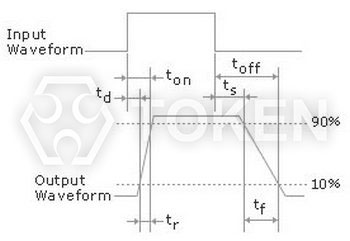
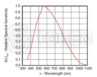
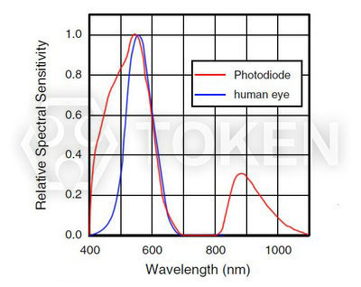
Most photodiodes and phototransistors have an epoxy filter function that increases the relative spectral sensitivity and makes it closer to the human eye's sensitivity. This is sometimes called the v(λ) curve. The part number contains the letter part of the FC with this epoxy resin. Figure 1 shows an ambient light sensor without epoxy filtering, and Figure 2 shows a sensor with epoxy filter. For this epoxy filter, the bandwidth (λ0.5) is reduced from 430 nm to 800 nm to 430 nm to 600 nm.
| Light Source | Illumination (Lux) | ALS Circuit Symbol |
| Moonlight | 0.1 | 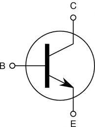 |
| 60W Light Bulb @1m | 50 | |
| 1W MES Light Bulb @0.1m | 100 | |
| Fluorescent Light | 500 | |
| Bright Sunshine | 30,000 |
Download Guide to Ambient Light Sensors in PDF file.
