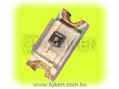
Chip Phototransistor, RoHS Compliant (PT-A8-AC-1206-850)
Chip Phototransistor, RoHS Compliant (PT-A8-AC-1206-850)
Chip Phototransistor precise light measurement across a wide spectrum of wavelengths.
A variety of inexpensive chip visible light sensor with a current output that is directly proportional towards the light level. They reveal excellent uniformity and linearity of performance with many types of light including tungsten filament, ambient, LED lights and fluorescent. The devices are supplied in SMD style (surface mounted device), especially designed to replace CdS cell as a result of the RoHS initiative.
Ambient light sensors (ALS) will also be known as illuminance or illumination sensors, photodetector, brightness sensors, photo transistor, optical sensors, or simply light sensors. One essential application for ALS technologies are mobile phones. Inside a mobile phone, the ALS enables automatic charge of display backlight brightness over an array of illumination conditions from the dark atmosphere to sunlight. This control significantly improves visibility and minimizes power consumption since LCD backlighting is able to take around 51% through the power within the input standby mode. Additionally, the ALS signal may be used to instruct the keypad LED driver to reduce keypad backlighting minimizing as much as 30% from the power within the input standby power mode.
Nowadays, designers convey more technology selections for ambient light sensors including photodiodes, photoelectric cells, phototransistors, and photo ICs. Each technologies have pros and cons. Among the key criteria for choosing an ALS is being able to identify the visible range of the human eye the 312nm to 1050nm wavelength is the 380nm - 780nm electromagnetic wave for visible light.
Chip phototransistors are silicon monolithic circuits with an integrated light-sensitive semiconductor photodiode — a PN junction which converts light into an electrical signal. The device have easily obtainable output current, small static current, fast response speed and stable performance. Suitable for all kinds of infrared light control, infrared radiation, infrared reflection, ultra-thin and multi-point infrared touch screen, high illumination or visible light interference strong products, and optical control infrared testing equipment.
Download complete specification Chip Phototransistor, RoHS Compliant (PT-A8-AC-1206-850) PDF.
- Good batch consistency, Small static current, Fast response speed and stable performance.
- No cadmium, lead free and other harmful substances, compliant with EU RoHS standards.
- Suitable for ultra-thin and multi-point infrared touch screen, replace the traditional CDs resistance.
- Suitable for all kinds of infrared light control, infrared radiation, infrared reflection,
applicable to all types of light control lighting products: such as small night Lights, lawn lights, solar lamps. - Suitable for all kinds of high illumination or visible light interference strong products, automatic adjustment background light:
such as LCD, mobile phone, camera, computer camera, installation control machine. - Control all kinds of optical control video control toys and All kinds of optical control infrared testing equipment.
- For the convenience of installation in all kinds of products in any position, different sizes are available upon request.
- Provide bright current / dark current (bright resistance / dark resistance) for the most suitable product.
Dimensions & Configurations (PT-A8-AC-1206-850) Unit: mm
|
||||||||||
| Part NO. | A (mm) | B (mm) | C (mm) | D (mm) | E (mm) | |||||
| PT-A8-AC-1206-850 | 3.2 ± 0.2 | 2.0 ± 0.2 | 1.5 ± 0.2 | 1.1 ± 0.2 | 0.6 ± 0.2 | |||||
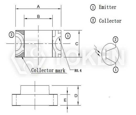
- The epoxy resin highest: 1.5mm max.
- Product images, plastic color of apperence, and all other information is for reference only, goods in-kind prevail.
- Short Lead—Collector Long Lead—Emitter.
Electro-Optical Characteristics (Ta=25°C) (PT-A8-AC-1206-850)
| Parameter | Symbol | Condition | Min. | Typ. | Max. | Unit |
| Peak Wavelength | λp | \ | - | 850 | - | nm |
| Spectral Response Bandwidth | λ | \ | 400 | - | 1100 | nm |
| Collector-Emitter Breakdown Voltage | Bvceo | Ice=100µA Ee=0mW/cm2 |
30 | - | - | V |
| Emitter-Base Breakdown Voltage | Bveco | Ice=100µA Ee=0mW/cm2 |
3 | - | - | V |
| Collector-Emitter Saturation Voltage | Vce (sat) |
Ice=2mA Ee=1mW/cm2 |
- | - | 0.4 | V |
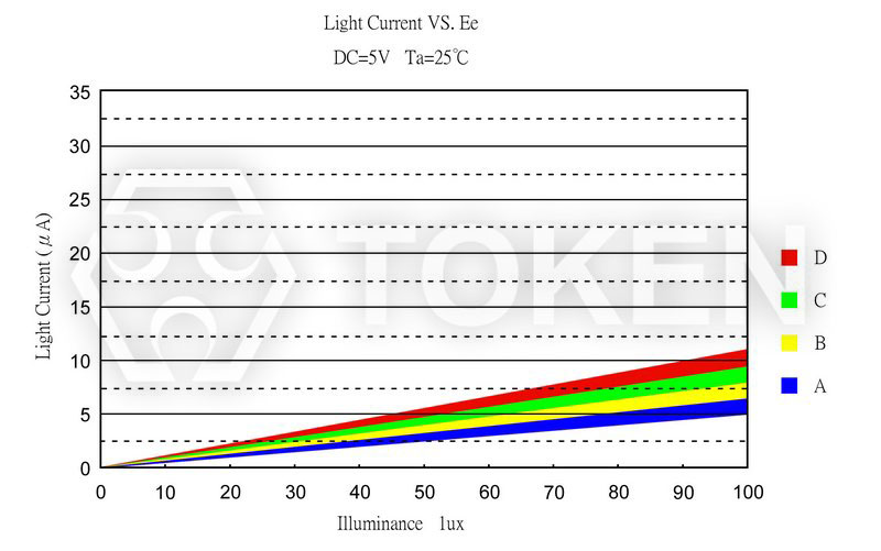
| Photo Current | IL(1) | Vcc=5V Ev=10Lux |
0.5 | 0.8 | 1.2 | μA |
| IL(2) | Vcc=5V Ev=30Lux |
1.5 | 2.4 | 3.6 | μA | |
| IL(3) | Vcc=5V Ev=100Lux |
5 | 8 | 12 | μA | |
| Collector Dark Current | Iceo | Vce=5V Ev=0Lux |
- | - | 0.1 | μA |
| Rise Time | tr | Vcc=5V Ice=1mA RL=1000Ω |
15 | us | ||
| Fall Time | tf | 15 | ||||
Shipping standards:
| Photo Current | Test conditions | A shift | B shift | C shift | D shift | X shift | Unit |
| Vce=5V Ev=10Lux |
/ | / | / | / | 0.5 ~ 1.2 | μA |
Absolute Maximum Ratings: (Ta=25°C) (PT-A8-AC-1206-850)
| Parameter | Symbol | Value | Unit |
| Collector-Emitter Voltage | VCEO | 30 | V |
| Emitter-Collector-Voltage | VECO | 3 | V |
| Power Dissipation | PC | 70 | mW |
| Operating Temperature Range | Topr | -25 ~ +85 | °C |
| Storage Temperature | Tstg | -40 ~ +100 | °C |
Relative Spectral Sensitivity vs. Wavelength (PT-A8-AC-1206-850)
|
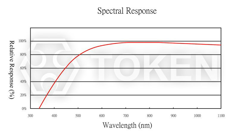
Photo Current vs. Illuminance (PT-A8-AC-1206-850)
|
Dark Current vs. Ambient Temperature P(PT-A8-AC-1206-850)
|
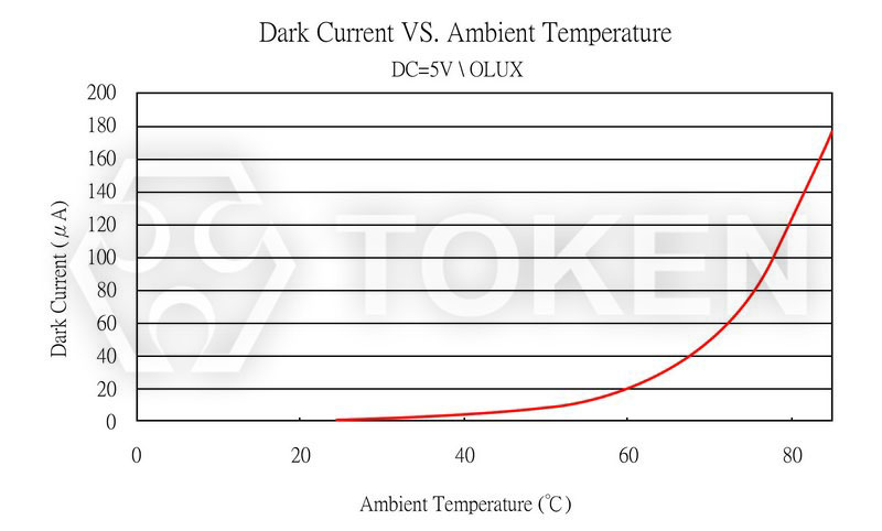
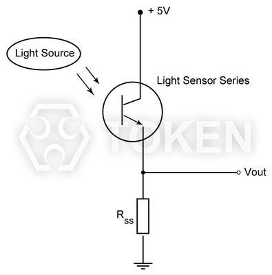
Photo Current Measurement Method - PT-A8-AC-1206-850
Mounting :
- While packages are on one circuit board, avoid mismatching in the thermal expansion of each component, generate cracks in the package and break the bonding wire.
Soldering :
- Do not immerse plastic parts in tin tank.
- During soldering, when adding thermal stress in a moisture absorbing state, moisture evaporates, swells and generates stress to the internal package.
- To avoid swellings and cracks in the surface of the package, followsoldering conditions below.
- Wave soldering method: 120°C < 60s、260°C < 5s.
- Manual soldering: 260°C < 5s、340°C < 3s.
Lead-forming and cuttings :
- Before soldering, perform lead forming at normal temperature.
- While forming or cutting the lead, stay the area at a distance of 5 mm or greater from the root of the lead.
- Avoid mounting which may cause force on the root of the lead.
Storage:
The sensor is incorporated in the transparent resin package. Because of its sensitivity to humidity, the package is moisture-proof. When storing the sensor, do as instructed below.
- Quickly use after opening. (within 2 days, below 30 °C/60 % R.H.).
- Once unpacked, use within three months, or keeping within a moisture-proof method, which include maintaining within a moisture-proof container with silica gels, is suggested for longterm safe-keeping.
- Very bad storage conditions may deteriorate solderability or characteristics, and defect the appearance. Recommended conditions of the storage place, temperature 0°C to 30 °C, humidity below 60% R.H. (Avoid freezingand dew condensation).
Cleaning:
- Do not wash with water to avoid corrosion.
- Under any circumstance, the cleaning time should be within 1 minute of normal temperature.
- Alcohol is recommended as a cleaning agent when cleaning products.
- If you use other cleaning agents, you need to confirm whether the cleaning agent will corrode the epoxy body.
- Freon can not be used as a cleaning agent.
- When cleaning products with ultrasonic cleaning, ultrasonic power and time should be less than 300W and 30 seconds, respectively.
- PCB and product can not touch the oscillator. Can not make the product on the PCB resonance.
- This model is static sensitive devices, so static electricity and surges can damage the product.
- To all the equipment, machines, tables, and the ground must be anti-static ground.
- Requires the use of anti-static wrist strap wear.
Order Codes (PT-A8-AC-1206-850)
| PT | - | A8 | - | AC | - | 1206 | - | 850 | ||||||||||||||||||
 | | | | | ||||||||||||||||||||||
|
|
|
|
|
||||||||||||||||||||||