Chip Phototransistors, SMD Ambient Light Sensors
SMD Phototransistor (Infrared-Blocking)
Thumbnail
Description
1
The (PT-B1-DC-0603-940) surface mounted infrared receiving light sensor features fast response speed, stable performance, low current loss in static, and anti-strong light interference.
Download (PT-B1-DC-0603-940) PDF
2
The (PT-IC-AC-3528-520) is a high-precision environment-friendly ambient light sensor. Optical IC with spectral response close to human eye sensitivity. Control all kinds of optical control video control toys and All kinds of optical control infrared testing equipment.
Download (PT-IC-BC-3528-550) PDF
SMD Phototransistor (Non Infrared-Blocking)
Thumbnail
Description
1
Chip phototransistors are silicon monolithic circuits with an integrated light-sensitive semiconductor photodiode — a PN junction which converts light into an electrical signal. Suitable for ultra-thin and multi-point infrared touch screen, replace the traditional CDs resistance.
Download (PT-A8-AC-1206-850) PDF
2
Ambient light sensors mimic the human eye with peak wavelength 520nm and 520nm, anti-infrared interference. Fast response speed and stable performance, Good batch consistency, Small static current.
Download (PT-IC-AC-3528-520) PDF
3
The (PTA1AC3528-850) is a sensor with near the human eye that measures the intensity of visible light. Suitable for all kinds of high illumination or visible light interference strong products, automatic adjustment background light.
Download (PT-A1-AC-3528-850) PDF
Light Sensors - Explanation Of Product Code
|
|
|
|
|
|
||||||||||||||||||||||||||||||||||||||||||||||||||||||||||||||||||||
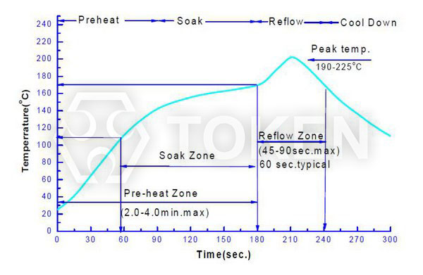
Recommended Reflow Chart
|
||||||||||
| Characteristic of Temperature Curve | Reference Settings | |||||||||
| Average Heating Speed (Tsmax to Tp) | Max. 3°C / Sec | |||||||||
| Preheating: Minimum Temperature | (Tsmin) | |||||||||
| Preheating: Maximum Temperature (Tsmax) | 150°C | |||||||||
| Preheating: Time (tsmin to tsmax) | 60 ~ 120 Sec | |||||||||
| Reflow Temperature: Temperature (TL) | 183°C | |||||||||
| Period of Reflow: Time (TL) | 60 ~ 150 Sec | |||||||||
| Peaking Temperature (TP) | 225°C | |||||||||
| Within the Actual Peak Temperature (tp) 5°C | 10 ~ 30 Sec | |||||||||
| Cooling speed | Max. 6°C / Sec | |||||||||
| 25°C Time required to rise to peak temperature | Max. 6 minutes | |||||||||
Token Chip Phototransistors - General Information
Mounting :
- While packages are on one circuit board, avoid mismatching in the thermal expansion of each component, generate cracks in the package and break the bonding wire.
Soldering :
- Do not immerse plastic parts in tin tank.
- During soldering, when adding thermal stress in a moisture absorbing state, moisture evaporates, swells and generates stress to the internal package.
- To avoid swellings and cracks in the surface of the package, followsoldering conditions below.
- Wave soldering method: 120°C < 60s、260°C < 5s.
- Manual soldering: 260°C < 5s、340°C < 3s.
Lead-forming and cuttings :
- Before soldering, perform lead forming at normal temperature.
- While forming or cutting the lead, stay the area at a distance of 5 mm or greater from the root of the lead.
- Avoid mounting which may cause force on the root of the lead.
Cleaning :
- Do not wash with water to avoid corrosion.
- Under any circumstance, the cleaning time should be within 1 minute of normal temperature.
- Alcohol is recommended as a cleaning agent when cleaning products.
- If you use other cleaning agents, you need to confirm whether the cleaning agent will corrode the epoxy body.
- Freon can not be used as a cleaning agent.
- When cleaning products with ultrasonic cleaning, ultrasonic power and time should be less than 300W and 30 seconds, respectively.
- PCB and product can not touch the oscillator. Can not make the product on the PCB resonance.
- This model is static sensitive devices, so static electricity and surges can damage the product.
- To all the equipment, machines, tables, and the ground must be anti-static ground.
- Requires the use of anti-static wrist strap wear.
Service life :
- It can be used for up to 100,000 hours at rated current and rated voltage.
Baking and dehumidification :
- Use instructions before soldering this product. After opening the original wrapper, product exposure and humid environment. Product may be damaged during soldering.
- Description of the storage: Products with exposure time exceeding the specified time must be baked according to the baking conditions listed below. The following downgrade table determines the maximum amount of time that this product can be exposed to the humidity and temperature conditions listed. (Unit: Day)
- Baking conditions: No need to bake all the products. Baking is required only if the following criteria are met:
- A: Products that have been removed from the original package;
- B: Exposure to humid environments over time which list in Relative Humidity Table.;
- C: Products that have not been soldered.
Reflow soldering of parts within one hours after baking, or immediately store the part in a container of relative humidity less than 20%. The product should be baked in its original reel under 60°C for 24 hours. The exposure time of the products after this baking process is again determined by the moisture sensitivity table above.
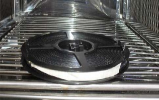
Figure 2Wrong baking style
| Temperature | Maximum Relative Humidity (%) | ||||||
| 30% | 40% | 50% | 60% | 70% | 80% | 90% | |
| 30°C | 9 | 5 | 4 | 3 | 1 | 1 | 1 |
| 25°C | 12 | 7 | 5 | 4 | 2 | 1 | 1 |
| 20°C | 17 | 9 | 7 | 6 | 2 | 2 | 1 |
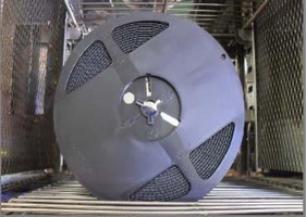
Figure 2The Right way to bake
Storage :
- Without opening the original wrapper, the recommended storage environment is: 5°C ~ 30°C, Humidity less 85%.
- After opening the original wrapper, the recommended storage environment is: 5°C ~ 30°C, Humidity less 60%.
- This product is humidity sensitive device. In order to avoid moisture absorption after unpackage, it is recommended that the opened packaging be stored in an airtight container with desiccant.
- After opening the package, the original should be used within 12 hours.
- If the desiccant fails or the device is exposed to air for more than 12 hours. Should be used for dehumidification treatment at 60°C / 24H.
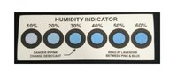
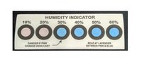
Use and description of Humidity Monitor card :
- The card with "Humiditor" in the bag is the humidity monitor card.
- If there is no humidity in the bag, then the color in the black circle of the monitor card is blue as shown in Figure (1).
- If humidity card "20%" corresponds to the black circle showing the color is pink, then bake and dehumidification the product as shown in Figure (2).
- Humidity card indicates packaging bag humidity conditions.
|
|
||||||||||||||||||||
Electrostatic Protection :
- Electrostatic and surge will cause changes in product characteristics, such as positive voltage dropping, etc.
The situation is serious, even damaging the product. - During the whole process (production, testing, packaging, etc.), who might contact with chip phototransistor,
do measures to prevent and eliminate static electricity. - All relevant equipment and machines should be properly grounded. Grounding AC resistance is less than 1.0 Ω,
the worktable needs to cushion surface resistance 106 Ω ~ 109 Ω Table Mat. - The ion fan must be installed on the environment and equipment that produce electrostatic easily.
- Operation process, operators need to use anti-static bracelet, anti-static cushion, anti-static overalls, work shoes, gloves, anti-static capacitors.
Packing format (Tape and reel) :
|
||||||||||
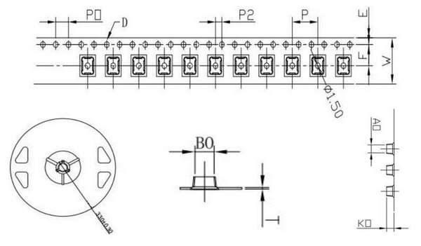
| ITEM | W | A0 | B0 | D | F | E | K0 | P0 | P2 | P | T |
| DIM | 12 | 3.0 | 3.7 | 1.5 | 5.5 | 1.75 | 2.6 | 4.0 | 2.0 | 8.0 | 0.35 |
| TOLE | ±0.3 | ±0.1 | ±0.1 | ±0.1 | ±0.1 | ±0.1 | ±0.1 | ±0.1 | ±0.1 | ±0.1 | ±0.05 |
Other Matters :
- The resin package of the Chip Light Sensor product is quite fragile. Do not scrape the encapsulated resin part with a hard, sharp object.
Should also be very careful when using tweezers to clamp the SMD Light Sensor. - Do not directly use the hand to take the Chip Light Sensor products.
The direct use of hand to get the chip phototransistor will not only pollute the surface of the chip packaging resin,
but also may be due to static factors such as chip product performance changes. - Do not exert excessive pressure on Chip Light Sensor, especially when Chips are in high temperature (for example, during reflow soldering).
Excessive pressure may directly affect the inner chip and the gold wire. - Chip phototransistor working environment and chip adaptation of the material sulfur elements and compounds can not exceed 100PPM.
- The module material cannot be stacked together and may damage the internal circuitry.
- Not available in PH<7 acidic sites.
PDF Catalogue :
Download Entire Light Sensors, Ambient Light Sensors in PDF file.