Flip Chip Network Resistor Array (FCR, RCA, RCN) Thick Film
Flip Chips (FCR, RCA, RCN) Introduction
Token makes Flip Chip, Resistor Networks, Chip Array a green old age.
Token has introduced precision surface-mount resistor networks, chip array, and flip-chips. Those no-lead packages are optimized to meet new automotive industry requirements for temperature and humidity, while offering high repeatability and stable performance for industrial, telecommunication, and consumer electronics.
Suitable for processing on automatic SMD assembly systems, those new devices are RoHS-compliant and compatible with lead (Pb)-free and tin/lead (Sn/Pb) reflow and vapor-phase soldering processes.
- The resistor flip chip configurations (FCR Series) are available in industry standard EIA0603, EIA0805, and EIA1206.
- Power Rating 1/10W, 1/8W, and 1/4W are available in max. voltage 100V, 300V, and 300V respectively.
- Resistance tolerance is tight to F(± 1%), J(± 5%) with resistance range 1Ω to 10MΩ.
- Its small 1.6mm by 3.2mm package enables the design of high-density circuits.
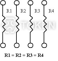
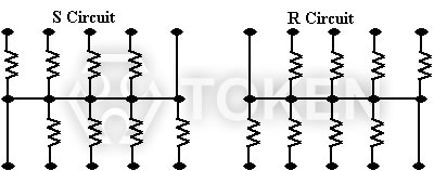
- The resistor chip array (RCA Series) offers a low cost when compared to using four high-precision resistors.
- The devices feature precision ratio tolerances to F(± 1%), G(± 2%), and J(± 5%) are available with resistance range 10Ω to 1MΩ.
- The (RCN) resistor networks offer a resistance range from 10Ω to 1MΩ at operating temperature range -55°C~+125°C.
- All devices offer power ratings of 1/16W at +70°C per resistor, custom configurations of the devices are available.
Full line products meet RoHS compliant. Detailed specifications, both mechanical and electrical, please contact our sales representative for more information. Downloads Complete PDF Specification Flip Chip Array Resistor Network Resistors.
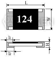
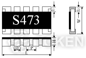
Surface Mount Flip Resistor Dimensions (Unit: mm) (FCR)
|
||||||
| Dimensions Type | L | W | H | L1 | L2 | |
| FCR 03 | 1.60 ± 0.10 | 0.80 ± 0.10 | 0.45 ± 0.10 | 0.30 ± 0.20 | 0.30 ± 0.20 | |
| FCR 05 | 2.00 ± 0.15 | 1.25 ± 0.15 | 0.50 ± 0.10 | 0.40 ± 0.20 | 0.35 ± 0.15 | |
| FCR 06 | 3.10 ± 0.15 | 1.55 ± 0.15 | 0.55 ± 0.10 | 0.50 ± 0.25 | 0.50 ± 0.25 | |
SMD Array Resistor Dimensions (Unit: mm) (RCA)
|
||||||||
| Dimensions Type | L | W | H | L1 | L2 | P | Q | |
| RCA03-4D (0603) | 3.2±0.2 | 1.6±0.15 | 0.5±0.1 | 0.30±0.15 | 0.35Max | 0.8±0.1 | 0.5±0.1 | |
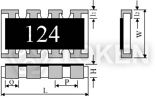
SMD Network Resistor Dimensions (Unit: mm) (RCN)
|
||||||||
| Dimensions Type | L | W | H | L1 | L2 | P | Q | |
| RCN06-10R RCN06-10S |
6.4 ± 0.2 | 3.1 ± 0.2 | 0.55 ± 0.1 | 0.5 ± 0.3 | 0.5 ± 0.2 | 1.27 ± 0.1 | 0.8 ± 0.2 | |
Electrical Specifications (FCR)
| Type | Power Rating at 70°C | Max. RCWV | Max. Overload Voltage | Resistance Tolerance(%) | Resistance Range (Ω) | Standard Resistance Values | |
| Min. | Max. | ||||||
| FCR03 | 1/10W | 50V | 100V | ± 1% (F) ± 5% (J) |
10Ω 1Ω |
1MΩ 10MΩ |
E-96 E-24 |
| FCR05 | 1/8W | 150V | 300V | ± 1% (F) ± 5% (J) |
10Ω 1Ω |
1MΩ 10MΩ |
E-96 E-24 |
| FCR06 | 1/4W | 200V | 300V | ± 1% (F) ± 5% (J) |
10Ω 1Ω |
1MΩ 10MΩ |
E-96 E-24 |
Electrical Specifications (RCA)
| Type | Rated Power at70°C | Max. Working Voltage | Max. Overload Voltage | T.C.R. (ppm/°C) | Resistance Range | Jumper Rated Current | Jumper Resistance Value | Operating Temperature Range | |
| F(±1%) E-96 |
G(±2%) J(±5%) E-24 |
||||||||
| RCA03-4D (0603) |
0.063 | 50V | 100V | ± 200 | 100Ω~470KΩ | 10Ω~1MΩ | 1A | 50mΩ MAX |
-55°C~+125°C |
Electrical Specifications (RCN)
| Type | Rated Power at70°C | Max. Working Voltage | Max. Overload Voltage | T.C.R. (ppm/°C) | Resistance Range | Number of Terminals |
Number of Elements |
Operating Temperature Range |
| J (±5%) E-12 | ||||||||
| RCN06-10R RCN06-10S |
1/16W | 50V | 100V | ±200 | 10Ω~1MΩ | 10 | 8 | -55°C~+125°C |
Environmental Characteristics (FCR, RCA, RCN)
| ITEM | SPECIFICATION | TEST METHOD |
| DC Resistance | J: ±5%, F: ±1% | JIS C 5202 5.1 |
| Temperature Coefficient of Resistance(TCR) |
J: ±200ppm/°C F: ±100ppm/°C |
JIS C 5202 5.2 / IEC 115-1 4.8.4.2 Test temperature:25°C → -55°C |
| Short Time Overload | J: ΔR≤ ± (2%+0.1Ω) F: ΔR≤ ± (1%+0.05Ω) |
JIS C 5202 5.5 / IEC 115-1 4.13 2.5xRated voltage (Max. Overload Voltage) for 5 sec. measure resistance after 30 minutes |
| Resistance to Solder Heat |
J: ΔR≤ ± (1%+0.1Ω) F: ΔR≤ ± (0.5%+0.05Ω) No mechanical damage |
JIS C 5202 6.4 / IEC 115-1 4.18 With 260 ± 5 °C for 10 ± 1 sec. |
| Solderability | Over 95% of termination must becovered with solder |
JIS C 5202 7.4 / IEC 115-1 4.17 After immersing flux, dip in the 235 ± 5°C molten solder bath for 2 ± 0.5 sec. |
| Temperature Cycle | J: ΔR≤ ± (1%+0.1Ω) F: ΔR≤ ± (0.5%+0.05Ω) No mechanical damage |
JIS C 5202 7.4 / IEC 115-1 4.19 Repeat 5 cycles as follow -55°C(30minutes)+25°C(10~15minutes) +125°C(30minutes)+25°C(10~15minutes) |
| Terminal Strength | ΔR≤ ± (0.5%+0.05Ω) No mechanical damage |
JIS C 5202 6.1 500g for 10 seconds |
| Load Life | J: ΔR≤ ± (3%+0.1Ω) F: ΔR≤ ± (1%+0.05Ω) |
JIS C 5202 7.10 / IEC 115-1 4.25.1 Permanent resistance change after 1000+48/-0 hours (1.5 hours ON,0.5hour OFF) at RCWV or Max. Keep the element at 70 ± 3°Cambient |
| Load Life Humidity | J: ΔR≤ ± (3%+0.1Ω) F: ΔR≤ ± (1%+0.05Ω) |
JIS C 5202 7.9 / IEC 115-1 4.24.2 Maintain the temperature of the element at 40 ± 2 °Cand 90~95% RH with the rated voltage applied. Cycle ON for 1.5hours and Off for 0.5hour for 1000+48/-0 hours. After one hour, measure the resistance value. |
| Intermittent Overload | ΔR≤ ± (5%+0.1Ω) No mechanical damage |
JIS C 5202 5.8 2.5xRated Voltage(Max. Overload Voltage), 1secON,25sec OFF, test 10,000 cycles |
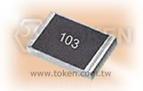
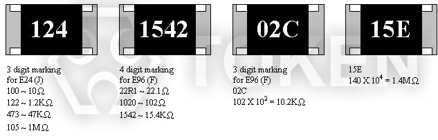
Marking (FCR, RCA, RCN)
|
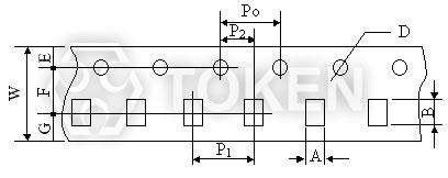
Tape Specifications (Unit: mm) (FCR, RCA, RCN)
|
|||||||||||
| TYPE | A | B | W | F | E | P1 | P2 | P0 | D | G | |
| FCR03 | 1.10±0.20 | 1.90±0.20 | 8.0±0.3 | 3.50±0.05 | 1.75±0.10 | 4.0±0.1 | 2.00±0.05 | 4.0±0.1 | 1.5±0.1 |
2.75 | |
| FCR05 | 1.65±0.20 | 2.45±0.20 | 8.0±0.3 | 3.50±0.05 | 1.75±0.10 | 4.0±0.1 | 2.00±0.05 | 4.0±0.1 | 1.5±0.1 |
2.75 | |
| FCR06 | 2.00±0.10 |
3.57±0.10 |
8.0±0.3 | 3.50±0.05 | 1.75±0.10 | 4.0±0.1 | 2.00±0.05 | 4.0±0.1 | 1.5±0.1 |
2.75 | |
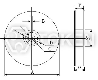
Reel Packaging (Unit: mm) (FCR, RCA, RCN)
|
|||||||||||
| Symbol | A | B | C | D | G | N | T | ||||
| Dimension | 178 ± 2.0 | 20 ± 0.5 | 13.0 ± 0.5 | 20 min. | 100 ± 1.5 | 80.0 ± 0.5 | 14.9 max. | ||||
Order Codes Flip SMD Resistors (FCR)
| FCR | 03 | 100 | J | TR | |||||||||||||||||||||||||||||||||
| 1 | 2 | 3 | 4 | 5 | |||||||||||||||||||||||||||||||||
|
|
|
|
|
|||||||||||||||||||||||||||||||||
Order Codes Resistor SMD Array (RCA)
| RCA | 03 | - | 4 | D | 101 | J | TR | |||||||||||||||||||||||||||||||||||||||
| 1 | 2 | 3 | 4 | 5 | 6 | 7 | ||||||||||||||||||||||||||||||||||||||||
|
|
|
|
|
|
|
||||||||||||||||||||||||||||||||||||||||
Order Codes SMD Resistor Networks (RCN)
| RCN | 06 | - | 10 | R | 103 | J | TR | ||||||||||||||||||||||||||||
| 1 | 2 | 3 | 4 | 5 | 6 | 7 | |||||||||||||||||||||||||||||
|
|
|
|
|
|
|
|||||||||||||||||||||||||||||