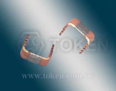
Alloy Sampling Shunt Current Sensing Resistors (FLU)
Sampling Alloy Shunts (FLU) Introduction
"Stamping" (FLU) precision shunt provides up to 7W power and a TCR as low as 40ppm.

Achieving the best detection results in the smallest space is one of the most common requirements of electronic design engineers for circuit systems. This is the advantage of the Token Electronics' stamping sampling shunt resistor technology.
Stamping type shunt resistor is also known as current detection alloy resistor, current sensing resistor, sampling shunts, current induction shunts.
The sampling resistance is divided into current sampling and voltage sampling. For current sampling, a resistor with smaller resistance value is connected in series, while for voltage sampling, a resistor with larger resistance value is connected in parallel. The function of sampling resistance is to convert current into voltage signal for current measurement. In the actual circuit, it is connected in series with the load resistor.
Designated the (FLU) through-hole devices offer a high current, flameproof alternative to conventional axial devices and flat chips for current-sense circuits where PC board space is at a premium. The open air resistor's footprint is reduced by extending the height of the device above the board, thus keeping the resistor element's "hot spot" safely off the PC board and providing for increased air circulation under it, which in turn provides increased heat dissipation and cooler operation. The structure adopts advanced alloy stamping and features high temperature resistance with low inductance.
The (FLU) offers a higher current load than conventional axial resistors and SMD resistors, with a wide range pitch of radial pins to choose from. Its rated power can be up to 1W ~7W, temperature coefficient as low as ±40ppm/°C, resistance tolerance accuracy ±1%, ±2%, and ±5%, resistance range as low as 0.1mΩ to 10mΩ.
The Low Ohmic Alloy Shunts (FLU) are available in bulk packaging and is RoHS compliant and lead free. For non-standard technical requirements and special applications, contact us with your specific needs.
Downloads complete specification PDF stamping shunt resistors.
- Sustain high temperature. Tolerance ±1%,±2% and ±5%.
- Low resistance 0.1mΩ to 10mΩ. Rated Power 1W ~ 7W with low inductance.
- Automotive electronics.Drive technology.
- Power Electronic, Home Appliance, Communication System
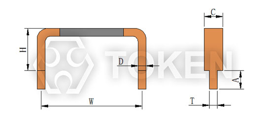
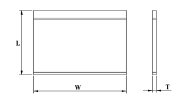
Dimensions - FLU (Unit:mm)
|
|||||||
| Resistance (mΩ) | W (mm) | C (mm) | D (mm) | H (mm) | A (mm) | T (mm) | |
| 0.1∼10 | 5∼30 | 10∼35 | 0.3∼3 | 5∼30 | 4±0.2 | 1.0±0.2 1.5±0.2 |
|
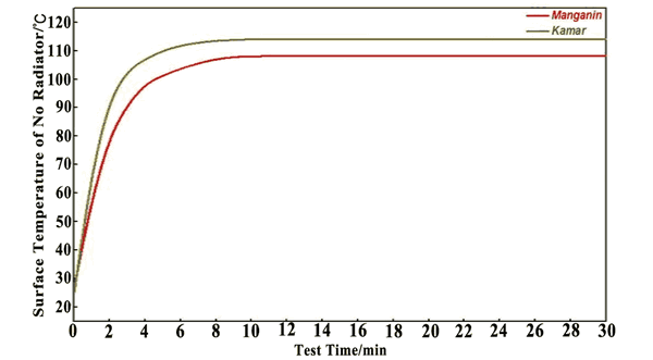
Surface Temperature Curve - FLU
|
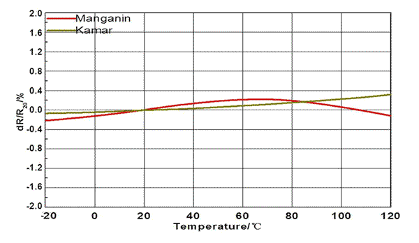
TCR Derating Curve - FLU
|
Environmental Characteristics - FLU
| Items | Methods | Requirement |
| Temperature Cycling | MIL-STD-202 1000 Cycles (-55°C to +125°C). Measurement at 24±2 hours after. |
±0.5% |
| High Temperature | MIL-STD-202 1000hrs. @T=125°. Unpowered. Measurement at 24±2 hours after. |
±0.5% |
| Moisture Resistance | MIL-STD-202 t=24 hrs/cycle. Note:Steps 7a & 7b not required. Measurement at 24±2 hours after. |
±0.5% |
| Biased Humidity | MIL-STD-202 1000hrs 85°C/85% RH. Note: Specified conditions: 10% of operating power. Measurement at 24±2 hours after. |
±0.5% |
| Operational Life | MIL-STD-202 Condition D Steady State TA=125°C at rated power. Measurement at 24±2 hours after. |
±0.5% |
| Solderability | J-STD-002C 245°C±5°C, 5s+0.5s/-0. |
95% Coverage Minimum. |
| Vibration | MIL-STD-202 5g's for 20 min, 12 cycles each of 3 orientations. Note: Use 8"X5" PCB. 031" thick 7" secure points on one long side and secure points at corners of opposite sides which parts mounted within 2 from any secure point. Test from 10-2000 Hz. Measurement at 24±2 hours after test conclusion. |
±0.5% |
| Resistance to Soldering Heat | MIL-STD-202 260°C±5°C, 10s±1s. Measurement at 24±2 hours after test conclusion. |
±0.5% |
| Short Time Overload | MIL-STD-202 5 × Rated power for 5s. Measurement at 24±2 hours after test conclusion. |
±0.5% |
| Thermal Shock | MIL-STD-202 -55°C/+125°C, 300 Cycles, Maximum transfer time 20s Dwell. |
±1% |
Derating Curve - FLU
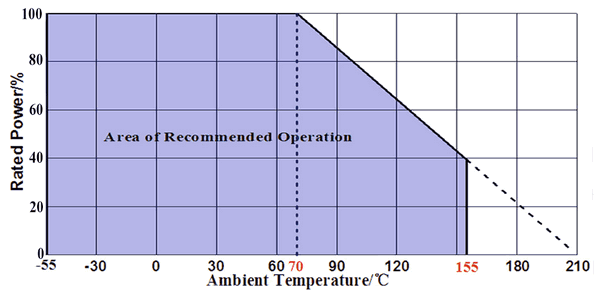 Rated power VS Ambient temperature (Derating Cruve) |
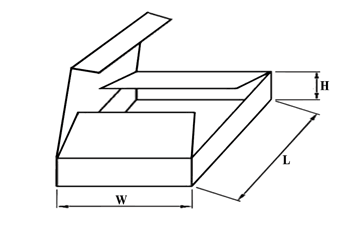
FLU - Internal Package
|
||||
| Type | L/mm | W/mm | T/mm | |
| P1 | 130 | 130 | 0.2 | |
| P2 | 160 | 160 | 0.2 | |
| P3 | 210 | 150 | 0.1 | |
FLU - External Package
|
||||
| Type | L/mm | W/mm | H/mm | |
| B1 | 170 | 120 | 50 | |
| B2 | 240 | 180 | 115 | |
| B3 | 230 | 170 | 200 | |
| B4 | 250 | 250 | 250 | |
| B5 | 300 | 300 | 300 | |
Alloy Current Sensing Resistors (FLU) Order Code
| FLU | 5 | 0m10 | F | ||||||||||||||||||||||||||||
 |
|
|
|
||||||||||||||||||||||||||||
|
|
|
|
||||||||||||||||||||||||||||
Note: Plating, tin dipping, or size, please can be required.