Thick-Film High Voltage Chip Resistors (HVR)
Chip High Voltage Resistor (HVR) Introduction
New (HVR) High-voltage chip resistors deliver power ratings up to 4 KV.
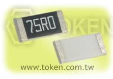
Token electronics has introduced a thick-film chip resistor series with wide resistance range from 10Ω to 100MΩ. The (HVR) series of surface mount resistors feature high-voltage operation in standard 0402, 0603, 0805, 1206, 2010 and 2512 package sizes, making them well ideal for automatic handling methods.
The (HVR) resistors offer high voltage, extended surge ratings. This pulse-withstanding chip resistor combines extended surge values with high-voltage ratings for high-power applications.
The (HVR) series are designed for use in high-voltage power supplies, circuit protection devices, medical equipment (defibrillators), military equipment (night vision cameras, x-ray equipment), automotive industry, and High Pulse Equipments.
Token's (HVR) series features high grade alumina substrate wrap-around terminations with an electroplated nickel barrier (Ni) with Edge Electrode (NiCr), and either tin/lead or RoHS-compliant matte tin finish. In addition, the overall robust construction allows the chip resistor to operate in harsh, high-voltage environments.
The (HVR) series feature tolerances of ±1%, and ±5%. Continuous voltage ratings are rated up to 3 KV, with maximum overload voltage to 4 KV. Power ratings for the HVR02(0402), HVR03(0603), HVR05(0805), HVR06(1206), HVR0A(2010) and HVR12(2512) resistors are 1/16W, 1/10W, 1/8W, 1/4W, 1/2W and 1W, respectively, with an operating temperature range of -55°C to +155°C. Custom specifications are available.
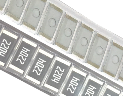
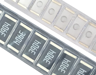
The (HVR) series are available in taping packaging and RoHS compliant.
For non-standard technical requirements and special applications, please contact us with your specific needs.
Download Complete PDF Specification Thick Film High Voltage Chip Resistors.
- Reduced size of final equipment, Miniature size HVR02(0402) available
- Excellent performance at high voltage, Higher component and equipment reliability
- Pb-free teurminations meet RoHS requirments, Thick film chips with highly reliable multiplayer electrode construction
- Automatic Equipment Controller, Inverter, Converters, Circuit Protection Devices
- High-Voltage Power Pupplies, Medical Equipment (Defibrillators, High Pulse Equipment)
- Printer Equipment, Consumer Product, Outdoor Equipments, Military Equipment (Night Vision Cameras, X-ray Equipment)
Construction & Dimensions (Unit: mm) (TCS)

High Voltage Thick Film Chip Resistor Construction (HVR)
|
| Type | L (Unit: mm) | W (Unit: mm) | T (Unit: mm) | D1 (Unit: mm) | D2 (Unit: mm) | Weight(g)/1000pcs |
| HVR02 (0402) | 1.00±0.05 | 0.50±0.05 | 0.35±0.05 | 0.20±0.10 | 0.20±0.10 | 0.620 |
| HVR03 (0603) | 1.60±0.10 | 0.80±0.10 | 0.45±0.10 | 0.30±0.20 | 0.30±0.20 | 2.042 |
| HVR05 (0805) | 2.00±0.10 | 1.25±0.10 | 0.50±0.10 | 0.35±0.20 | 0.40±0.20 | 4.368 |
| HVR06 (1206) | 3.10±0.10 | 1.55±0.10 | 0.55±0.10 | 0.50±0.25 | 0.50±0.20 | 8.947 |
| HVR0A (2010) | 5.00±0.10 | 2.50±0.15 | 0.55±0.10 | 0.60±0.25 | 0.50±0.20 | 24.241 |
| HVR12 (2512) | 6.35±0.10 | 3.10±0.15 | 0.55±0.10 | 0.60±0.25 | 0.50±0.20 | 39.448 |
Recommend Land Pattern (Unit: mm) (HVR)

Recommend Land Pattern (HVR) |
Codes | A (mm) | B (mm) | C (mm) |
| HVR02 (0402) | 0.50 | 0.45 | 0.60±0.2 |
| HVR03 (0603) | 0.90 | 0.60 | 0.90±0.2 |
| HVR05 (0805) | 1.20 | 0.70 | 1.30±0.2 |
| HVR06 (1206) | 2.00 | 0.90 | 1.60±0.2 |
| HVR0A (2010) | 3.80 | 0.90 | 2.80±0.2 |
| HVR12 (2512) | 3.80 | 1.60 | 3.50±0.2 |
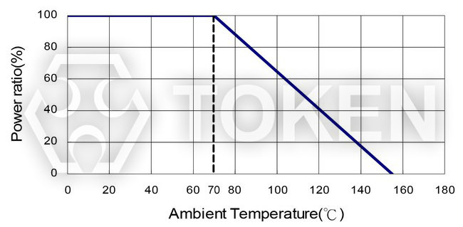
Power Derating Curve (HVR)
|
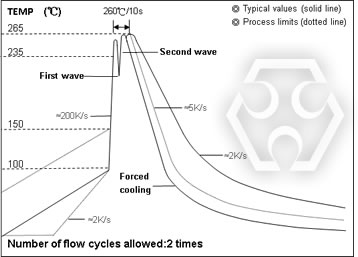
Soldering Condition (HVR)
|
|
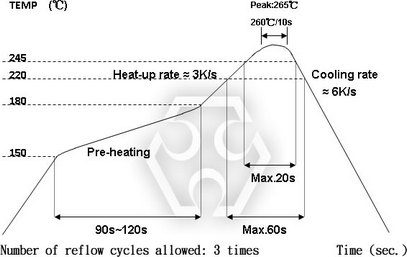
- Time of IR reflow soldering at maximum temperature point 260°C:10s
- Time of wave soldering at maximum temperature point 260°C:10s
- Time of soldering iron at maximum temperature point 410°C:5s
Standard Electrical Specifications (HVR)
| Type | Power Rating at 70°C | Operating Temp. Range | Max Operating Voltage | Max Overloading Voltage | Resistance Tolerance | Resistance Range | TCR |
| HVR02 (0402) |
1/16W | -55 ~ +155°C | 100V | 200V | ±1.0%, ±5.0% | 39KΩ~1MΩ | ±100PPM/°C |
| ±1.0% | 1.02MΩ~10MΩ | ±200PPM/°C | |||||
| ±5.0% | 1.1MΩ~20MΩ | ±200PPM/°C | |||||
| ±5.0% | 22MΩ~100MΩ | ±400PPM/°C | |||||
| HVR03 (0603) |
1/10W | -55 ~ +155°C | 200V | 400V | ±1.0%, ±5.0% | 56KΩ~1MΩ | ±100PPM/°C |
| ±1.0% | 1.02MΩ~10MΩ | ±200PPM/°C | |||||
| ±5.0% | 1.1MΩ~20MΩ | ±200PPM/°C | |||||
| ±5.0% | 22MΩ~100MΩ | ±400PPM/°C | |||||
| HVR05 (0805) |
1/8W | -55 ~ +155°C | 400V | 800V | ±1.0%, ±5.0% | 100KΩ~1MΩ | ±100PPM/°C |
| ±1.0% | 1.02MΩ~10MΩ | ±200PPM/°C | |||||
| ±5.0% | 1.1MΩ~20MΩ | ±200PPM/°C | |||||
| ±5.0% | 22MΩ~100MΩ | ±400PPM/°C | |||||
| HVR06 (1206) |
1/4W | -55 ~ +155°C | 500V | 1000V | ±1.0%, ±5.0% | 100KΩ~1MΩ | ±100PPM/°C |
| ±1.0% | 1.02MΩ~10MΩ | ±200PPM/°C | |||||
| ±5.0% | 1.1MΩ~20MΩ | ±200PPM/°C | |||||
| ±5.0% | 22MΩ~100MΩ | ±400PPM/°C | |||||
| HVR0A (2010) |
1/2W | -55 ~ +155°C | 2000V | 3000V | ±1.0%, ±5.0% | 51KΩ~1MΩ | ±100PPM/°C |
| ±1.0% | 1.02MΩ~10MΩ | ±200PPM/°C | |||||
| ±5.0% | 1.1MΩ~20MΩ | ±200PPM/°C | |||||
| ±5.0% | 22MΩ~100MΩ | ±400PPM/°C | |||||
| HVR12 (2512) |
1W | -55 ~ +155°C | 3000V | 4000V | ±1.0%, ±5.0% | 30KΩ~1MΩ | ±100PPM/°C |
| ±1.0% | 1.02MΩ~10MΩ | ±200PPM/°C | |||||
| ±5.0% | 1.1MΩ~20MΩ | ±200PPM/°C | |||||
| ±5.0% | 22MΩ~100MΩ | ±400PPM/°C |
- Lower Resistance:(1~10)Ω.
- Operating Voltage =√ ( P * R ) , or Max. Operating Voltage listed in above table whichever is lower.
- Overloading Voltage = 2.5*√ ( P * R ) , or Max. Overloading Voltage listed in above table whichever is lower.
- Optional specifications can be required.
Environmental Characteristics (HVR)
| Item | Specification | Test Method | |
| Tol. 1% | Tol. 5% | ||
| Dry Heat | ±(1%+0.05Ω) | ±(1.5%+0.10Ω) | JIS-C-5201-1 4.23 IEC-60115-1 4.23.2 At +155°C for 1000 hrs. |
| Endurance | ±(2%+0.10Ω) | ±(3%+0.10Ω) | JIS-C-5201-1 4.25 IEC-60115-1 4.25.1 70±2°C, Max. working voltage for 1000 hrs with 1.5 hrs “ON” and 0.5 hrs “OFF”. |
| Bending Strength | ±(1%+0.05Ω) | ±(1%+0.05Ω) | JIS-C-5201-1 4.33 IEC-60115-1 4.33 Bending once for 5 seconds, 2010, 2512 sizes: 2mm, other sizes:3mm. |
| Short Time Overload | ±(1%+0.05Ω) | ±(2%+0.05Ω) | JIS-C-5201-1 4.13 IEC-60115-1 4.13 RCWV*2.5 or Max Overloading Voltagewhichever is lower for 5 seconds. |
| Damp Heat with Load | ±(2%+0.10Ω) | ±(3%+0.10Ω) | JIS-C-5201-1 4.24 IEC-60115-1 4.24 40±2°C, 90~95% R.H. Max. working voltage for 1000 hrs with 1.5 hrs “ON” and 0.5 hrs “OFF”. |
| Resistance to Soldering Heat | ±(0.5%+0.05Ω) | ±(1%+0.05Ω) | JIS-C-5201-1 4.18 IEC-60115-1 4.18 260±5°C for 10 seconds. |
| Rapld Change of Temperature | ±(0.5%+0.05Ω) | ±(1%+0.05Ω) | JIS-C-5201-1 4.19 IEC-60115-1 4.19 -55°C to +155°C, 5 cycles. |
| Temperature Coefficient of Resistance | AS Spec | JIS-C-5201-1 4.8 IEC-60115-1 4.8 -55°C ~ +125°C, 25°C is the reference temperature. |
|
| Insulation Resistance | ≥10GΩ | JIS-C-5201-1 4.6 IEC-60115-1 4.6 Max. overload voltage for 1 minute. |
|
| Solderability | 95% Min. coverage | JIS-C-5201-1 4.17 IEC-60115-1 4.17 245±5°C for 3 seconds. |
|
| Voltage Proof | No breakdown or flashover | JIS-C-5201-1 4.7 IEC-60115-1 4.7 HVR02: 150V for 1 minute; HVR03: 300V for 1 minute; HVR05/HVR06/HVR0A/HVR12: 500V for 1 minute |
|
| Leaching | Individual leaching area ≤5% total leaching area ≤10% |
JIS-C-5201-1 4.18 IEC-60068-2-58 8.2.1 260±5°C for 30 seconds. |
|
- Rated continuous Working Voltage (RCWV) = √ Power Rating × Resistance Value (Ω)or Max. Operating voltage whichever is lower.
- Storage Temperature: 15~28°C; Humidity < 80%RH;
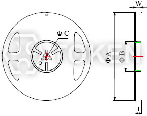
Packaging Quantity & Reel Specifications (Unit: mm) (HVR)
|
||||||||||
| Codes | Packaging Quantity (KPcs) | Tape Width | Reel Diameter | ΦA (mm) | ΦB (mm) | ΦC (mm) | W (mm) | T (mm) | ||
| HVR02 |
Paper
|
10K | 8mm | 7 inch | 178.5±1.5 | 60+1/-0 | 13.0±0.2 | 9.0±0.5 | 12.5±0.5 | |
| 20K | 8mm | 10 inch | 254±1 | 100±0.5 | 13.0±0.2 | 9.5±0.5 | 13.5±0.5 | |||
| 40K | 8mm | 13 inch | 330±1 | 100±0.5 | 13.0±0.2 | 9.5±0.5 | 13.5±0.5 | |||
| HVR03 HVR05 HVR06 |
Paper
|
5K | 8mm | 7 inch | 178.5±1.5 | 60+1/-0 | 13.0±0.2 | 9.0±0.5 | 12.5±0.5 | |
| 10K | 8mm | 10 inch | 254±1 | 100±0.5 | 13.0±0.2 | 9.5±0.5 | 13.5±0.5 | |||
| 20K | 8mm | 13 inch | 330±1 | 100±0.5 | 13.0±0.2 | 9.5±0.5 | 13.5±0.5 | |||
| HVR0A HVR12 |
Embossed
|
4K | 12mm | 7 inch | 178.5±1.5 | 60+1/-0 | 13.0±0.5 | 13.0±0.5 | 15.5±0.5 | |
| 8K | 12mm | 10 inch | 250±1 | 62±0.5 | 13.0±0.5 | 12.5±0.5 | 16.5±0.5 | |||
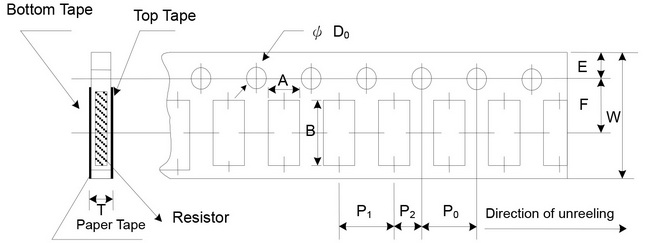
Paper Tape Specifications (Unit: mm) (HVR)
|
|||||||||||
| Codes | A (mm) | B (mm) | W (mm) | E (mm) | F (mm) | P0 (mm) | P1 (mm) | P2 (mm) | ΦD0 (mm) | T (mm) | |
| HVR02 | 0.65±0.10 | 1.15±0.10 | 8.0±0.20 | 1.75±0.10 | 3.50±0.05 | 4.00±0.10 | 2.00±0.05 | 2.00±0.05 | 1.50+0.1,-0 | 0.45±0.10 | |
| HVR03 | 1.10±0.10 | 1.90±0.1 | 8.0±0.2 | 1.75±0.1 | 3.50±0.05 | 4.00±0.10 | 4.00±0.05 | 2.00±0.05 | 1.50+0.1,-0 | 0.70±0.1 | |
| HVR05 | 1.60±0.10 | 2.40±0.2 | 8.0±0.2 | 1.75±0.1 | 3.50±0.05 | 4.00±0.10 | 4.00±0.05 | 2.00±0.05 | 1.50+0.1,-0 | 0.85±0.1 | |
| HVR06 | 1.90±0.10 | 3.50±0.2 | 8.0±0.2 | 1.75±0.1 | 3.50±0.05 | 4.00±0.10 | 4.00±0.05 | 2.00±0.05 | 1.50+0.1,-0 | 0.85±0.1 | |
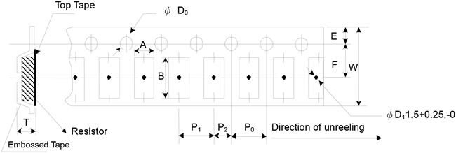
Emboss Plastic Tape Specifications (Unit: mm) (HVR)
|
|||||||||||
| Codes | A (mm) | B (mm) | W (mm) | E (mm) | F (mm) | P0 (mm) | P1 (mm) | P2 (mm) | ΦD0 (mm) | T (mm) | |
| HVR0A | 2.8±0.10 | 5.5±0.10 | 12.0±0.3 | 1.75±0.1 | 5.5±0.05 | 4.00±0.10 | 4.00±0.1 | 2.00±0.05 | 1.50+0.1, -0 | 1.2+0 | |
| HVR12 | 3.5±0.10 | 6.7±0.10 | 12.0±0.3 | 1.75±0.1 | 5.5±0.05 | 4.00±0.10 | 4.00±0.1 | 2.00±0.05 | 1.50+0.1, -0 | 1.2+0 | |
Order Codes (HVR)
| HVR | 03 | J | TR | E | V | 1003 | |||||||||||||||||||||||||||||||||||||||||||||||||||||||||||||||||
 |
|
|
|
|
|
|
|||||||||||||||||||||||||||||||||||||||||||||||||||||||||||||||||
|
|
|
|
|
|
|
|||||||||||||||||||||||||||||||||||||||||||||||||||||||||||||||||
0805~2512 4 digits marking for Example Marking
| Resistance | 100Ω | 2.2KΩ | 10KΩ | 49.9KΩ | 100KΩ | 1MΩ |
| Marking | 1000 | 2201 | 1002 | 4992 | 1003 | 1004 |
0603: 3 digits Marking E24 Nominal Table
| E24 code | 10 | 11 | 12 | 13 | 15 | 16 | 18 | 20 | 22 | 24 | 27 | 30 | 33 | 36 | 39 | 43 | 47 | 51 | 56 | 62 | 68 | 75 | 82 | 91 |
- Example: 101=100Ω 102=1KΩ (1st and 2nd are E24 code and 3rd code is multiplier)
- Resistance tolerance 1% for 0603: 3 digits marking in E96 (E96 series except E24 series)
- Digits marking for Example: 13C=13K3Ω; 68B=4K99Ω; 68X=49.9Ω
Marking Table E96 Nominal Table
| code | 02 | 03 | 04 | 06 | 07 | 08 | 09 | 10 | 11 | 13 | 14 | 15 | 16 | 17 | 19 | 20 | 21 | 22 | 23 | 24 | 25 | 26 | 27 |
| E96 | 102 | 103 | 107 | 113 | 115 | 118 | 121 | 124 | 127 | 133 | 137 | 140 | 143 | 147 | 154 | 158 | 162 | 165 | 169 | 174 | 178 | 182 | 187 |
| code | 28 | 29 | 31 | 32 | 33 | 34 | 35 | 36 | 37 | 38 | 39 | 40 | 41 | 42 | 43 | 44 | 45 | 46 | 47 | 48 | 49 | 50 | 51 |
| E96 | 191 | 196 | 205 | 210 | 215 | 221 | 226 | 232 | 237 | 243 | 249 | 255 | 261 | 267 | 274 | 280 | 287 | 294 | 301 | 309 | 316 | 324 | 332 |
| code | 52 | 53 | 54 | 55 | 56 | 57 | 58 | 59 | 60 | 61 | 62 | 63 | 64 | 65 | 66 | 67 | 68 | 69 | 70 | 71 | 72 | 73 | 74 |
| E96 | 340 | 348 | 357 | 365 | 374 | 383 | 392 | 402 | 412 | 422 | 432 | 442 | 453 | 464 | 475 | 487 | 499 | 511 | 523 | 536 | 549 | 562 | 576 |
| code | 75 | 76 | 77 | 78 | 79 | 80 | 81 | 82 | 83 | 84 | 86 | 87 | 88 | 89 | 90 | 91 | 92 | 93 | 94 | 95 | 96 | ||
| E96 | 590 | 604 | 619 | 634 | 649 | 665 | 681 | 698 | 715 | 732 | 768 | 787 | 806 | 825 | 845 | 866 | 887 | 909 | 931 | 953 | 976 |
Multiplier E96 Marking
| Code | A | B | C | D | E | F | X | Y |
| Multiplier | 100 | 101 | 102 | 103 | 104 | 105 | 10-1 | 10-2 |