Withstanding Pulse Load Chip Resistors (PWR)
Pulse Withstanding Resistor (PWR) Introduction
Token (PWR) Pulse Withstanding Chip Resistors provide 50 percent increase in power dissipation.
As electronic design engineers have increased the power density of their equipment, the demand for smaller surface mount single-chip circuit protection resistors has also increased. Token developed the PWR Series resistors to provide an economical alternative to bulky molded wirewound components or multi-chip solutions while saving both PC board space and manufacturing costs.
To meet the increased demand for the PWR Series resistors, Token has developed a series of pulse withstanding chip resistors with improved power ratings in reduced surface mounted sizes. Designated the PWR Series, the SMD resistors deliver up to 50 percent higher power ratings than conventional surface mount resistors - up to 1.5W in a standard 2512 size chip.
Token is able to boost this power rating up to 50 percent through a combination of proprietary power film materials and advanced manufacturing processes. The PWR Series Resistors are available in four standard sizes (0603, 0805, 1206, 1210, 2010 and 2512) with power ratings from 0.125W to 1.5W, and maximum operating voltage ratings for 100V to 500V. Resistance range is from 10 Ω to 20 MΩ, with tolerance tight to 0.5 percent. The PWR meets restriction of hazardous substances RoHS directive and RoHS compliance.
Along with the increased power ratings, the PWR Series resistors also feature high surge and high voltage ratings, making them extremely stable in demanding surge and pulse environments. The PWR Series chip resistors are specified for use in power supplies, circuit protection devices, portable battery chargers, motor controls and line-powered equipment.
Token will also produce devices outside these specifications to meet specific customer requirements, please contact our sales for more information.
Download complete pdf specification Chip Pulse Withstanding Resistors (PWR).
- Excellent Pulse Withstanding Performance.
- High Power Rating, Tolerance from ±0.5% ~ ±5%.
- Improved Working Voltage Ratings, Standard Package sizes 0603~2512.
- Portable Battery Chargers, Medical Devices.
- Metering (Testing/Measurement), Circuit Protection Devices.
- Diagnostic Equipment, ndustrial Controls, LCD Video Monitors.
- Power Supplies, Motor Controls and Line-Powered Equipment.
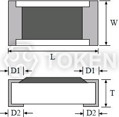
Dimensions (Unit: mm) (PWR)
|
|||||||
| Codes | L (Unit: mm) | W (Unit: mm) | T (Unit: mm) | D1 (Unit: mm) | D2 (Unit: mm) | Weight (g)/1000pcs | |
| PWR03 (0603) | 1.60±0.10 | 0.80±0.10 | 0.45±0.10 | 0.30±0.20 | 0.30±0.20 | 2,042 | |
| PWR05 (0805) | 2.00±0.10 | 1.25±0.10 | 0.50±0.10 | 0.35±0.20 | 0.40±0.25 | 4,368 | |
| PWR06 (1206) | 3.10±0.10 | 1.55±0.10 | 0.55±0.10 | 0.50±0.25 | 0.50±0.20 | 8,947 | |
| PWR13 (1210) | 3.10±0.10 | 2.60±0.15 | 0.55±0.10 | 0.50±0.25 | 0.50±0.20 | 15,959 | |
| PWR10 (2010) | 5.00±0.10 | 2.50±0.15 | 0.55±0.10 | 0.60±0.25 | 0.50±0.20 | 24,241 | |
| PWR12 (2512) | 6.35±0.10 | 3.10±0.15 | 0.55±0.10 | 0.60±0.25 | 0.50±0.20 | 39,448 | |
Recommend Land Pattern (Unit: mm) (PWR)
|
||||
| Codes | A (mm) | B (mm) | C (mm) | |
| PWR03 (0603) | 0.90 | 0.60 | 0.90 | |
| PWR05 (0805) | 1.20 | 0.70 | 1.30 | |
| PWR06 (1206) | 2.00 | 0.90 | 1.60 | |
| PWR13 (1210) | 2.00 | 0.90 | 2.80 | |
| PWR10 (2010) | 3.80 | 0.90 | 2.80 | |
| PWR12 (2512) | 3.80 | 1.60 | 3.50 | |

Standard Electrical Specifications (PWR)
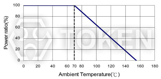
| Type | Power Rating at 70°C |
Operating Temp. Range | Max Operating Voltage | Max Overloading Voltage | Resistance Tolerance (%) |
Resistance Range (Ω) |
TCR PPM/°C |
| PWR03 (0603) | 1/10W | -55 ~ +155°C | 50V | 100V | ±0.5% | 10Ω~294Ω | ±200 |
| ±1%, ±5% | 1Ω~294Ω | ±200 | |||||
| ±0.5%, ±1%, ±5% | 300Ω~1MΩ | ±100 | |||||
| PWR05 (0805) | 1/8W | -55 ~ +155°C | 150V | 300V | ±0.5% | 10Ω~294Ω | ±200 |
| ±1%, ±5% | 1Ω~294Ω | ±200 | |||||
| ±0.5%, ±1%, ±5% | 300Ω~20MΩ | ±100 | |||||
| PWR06 (1206) | 1/3W | -55 ~ +155°C | 200V | 400V | ±0.5% | 10Ω~20Ω | ±200 |
| ±1%, ±5% | 1Ω~20Ω | ±200 | |||||
| ±0.5%, ±1%, ±5% | 20.5Ω~20MΩ | ±100 | |||||
| PWR13 (1210) | 1/2W | -55 ~ +155°C | 200V | 400V | ±0.5% | 10Ω~20Ω | ±200 |
| ±1%, ±5% | 1Ω~20Ω | ±200 | |||||
| ±0.5%, ±1%, ±5% | 20.5Ω~20MΩ | ±100 | |||||
| PWR10 (2010) | 3/4W | -55 ~ +155°C | 400V | 800V | ±0.5% | 10Ω~20Ω | ±200 |
| ±1%, ±5% | 1Ω~20Ω | ±200 | |||||
| ±0.5%, ±1%, ±5% | 20.5Ω~20MΩ | ±100 | |||||
| PWR12 (2512) | 1.5W | -55 ~ +155°C | 500V | 1000V | ±0.5% | 10Ω~20Ω | ±200 |
| ±1%, ±5% | 1Ω~20Ω | ±200 | |||||
| ±0.5%, ±1%, ±5% | 20.5Ω~20MΩ | ±100 |
- Lower Resistance:(1~10)Ω.
- Operating Voltage =√ ( P * R ) , or Max. Operating Voltage listed in above table whichever is lower.
- Overloading Voltage = 2.5*√ ( P * R ) , or Max. Overloading Voltage listed in above table whichever is lower.
- Optional specifications can be required.
High Power Rating Electrical Specifications (PWR)
| Type | Power Rating at 70°C |
Operating Temp. Range | Max Operating Voltage | Max Overloading Voltage | Resistance Tolerance (%) |
Resistance Range (Ω) |
TCR PPM/°C |
| PWR03 (0603) | 1/8W, 1/5W | -55 ~ +155°C | 50V | 100V | ±0.5% | 10Ω~294Ω | ±200 |
| ±1%, ±5% | 1Ω~294Ω | ±200 | |||||
| ±0.5%, ±1%, ±5% | 300Ω~1MΩ | ±100 | |||||
| PWR05 (0805) | 1/4W | -55 ~ +155°C | 150V | 300V | ±0.5% | 10Ω~294Ω | ±200 |
| ±1%, ±5% | 1Ω~294Ω | ±200 | |||||
| ±0.5%, ±1%, ±5% | 300Ω~20MΩ | ±100 | |||||
| PWR06 (1206) | 1/2W | -55 ~ +155°C | 200V | 400V | ±0.5% | 10Ω~20Ω | ±200 |
| ±1%, ±5% | 1Ω~20Ω | ±200 | |||||
| ±0.5%, ±1%, ±5% | 20.5Ω~20MΩ | ±100 | |||||
| PWR10 (2010) | 1W | -55 ~ +155°C | 400V | 800V | ±0.5% | 10Ω~20Ω | ±200 |
| ±1%, ±5% | 1Ω~20Ω | ±200 | |||||
| ±0.5%, ±1%, ±5% | 20.5Ω~20MΩ | ±100 |
- Lower Resistance:(1~10)Ω.
- Operating Voltage =√ ( P * R ) , or Max. Operating Voltage listed in above table whichever is lower.
- Overloading Voltage = 2.5*√ ( P * R ) , or Max. Overloading Voltage listed in above table whichever is lower.
- Optional specifications can be required.
Environmental Characteristics (PWR)
|
||||
| Test Item | Specification | Test Method | ||
| Short Time Overload | ±0.5% | JIS-C-5201-1 4.13 IEC-60115-1 4.13 RCWV*2.5 or Max Overloading Voltage whichever is lower for 5 seconds |
||
| Leaching | Individual leaching area ≥5% Total leaching area ≥10% |
JIS-C-5201-1 4.18 IEC-60068-2-58 8.2.1 -55°C~155°C, 5 cycles |
||
| Temperature Coefficient of Resistance | As Spec. | JIS-C-5201-1 4.8 IEC-60115-1 4.8 +25/-55/+25/+125/+25°C |
||
| Load Life (Endurance) |
±(1%+0.05Ω) | JIS-C-5201-1 4.25 IEC-60115-1 4.25.1 RCWV, 70°C, 1.5 hours ON, 0.5 hours OFF, total 1000 hours |
||
| Humidity (Steady State) (Damp Heat with Load) |
±(0.5%+0.05Ω) | JIS-C-5201-1 4.24 IEC-60115-1 4.24 40±2°C, 90~95%RH, RCWV 1.5 hours ON, 0.5 hours OFF, total 1000 hours |
||
| Resistance to Dry Heat | ±0.5% | JIS-C-5202-7.2 96 hours @ +155°C without load |
||
| Low Temperature Operation | ±0.5% | JIS-C-5202-7.1 1hour,-65°C followed by 45 minutes of RCWV |
||
| Dry Heat | ±(0.5%+0.05Ω) | JIS-C-5201-1 4.23 IEC-60115-1 4.23.2 at +155°C for 1000 hrs. 2010, 2512 sizes: 2mm; Other sizes: 3mm |
||
| Bending Strength | ±(1%+0.05Ω) | JIS-C-5201-1 4.33 IEC-60115-1 4.33 Bending once for 5 seconds. 2010, 2512 sizes: 2mm; Other sizes: 3mm |
||
| Resistance to Soldering Heat | ±(0.5%+0.05Ω) | JIS-C-5201-1 4.18 IEC-60115-1 4.18 260±5°C, 10±1seconds |
||
| Solderability | 95% min coverage | JIS-C-5201-1 4.17 IEC-60115-1 4.17 245°C±5°C for 3 seconds |
||
| Dielectric Withstand Voltage (Voltage Proof) |
No breakdown or flashover | JIS-C-5201-1 4.7 IEC-60115-1 4.7 1.42 times Max. Operating Voltage for 1 minute |
||
| Insulation Resistance | >10GΩ | JIS-C-5201-1 4.6 IEC-60115-1 4.6 Max. Overload Voltage for 1 minute |
||
- Storage Temperature: 25±3°C; Humidity: <80%RH.
- Rated continuous Working Voltage (RCWV) =√ Power Rating × Resistance Value (Ω)or Max. Operating voltage whichever is lower.
- Storage Temperature: 15°C~28°C; Humidity < 80%RH.
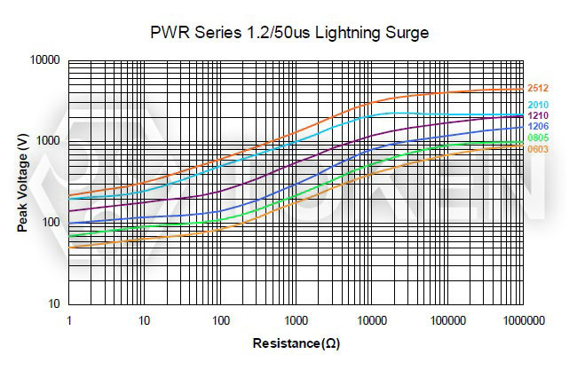
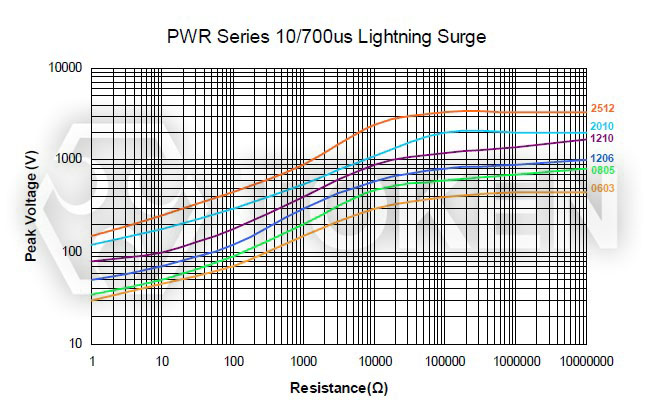
Lightning Surge of Pulse Withstanding Chip Resistor (PWR)
|
|||
| Note: | Lightning Surge of Pulse Withstanding Chip Resistors are tested in accordance with IEC 60 115-1 using both 10/700μs and 1.2/50μs pulse shapes. The limit of acceptance is a shift in resistance of less than 1% from the initial value. |
||
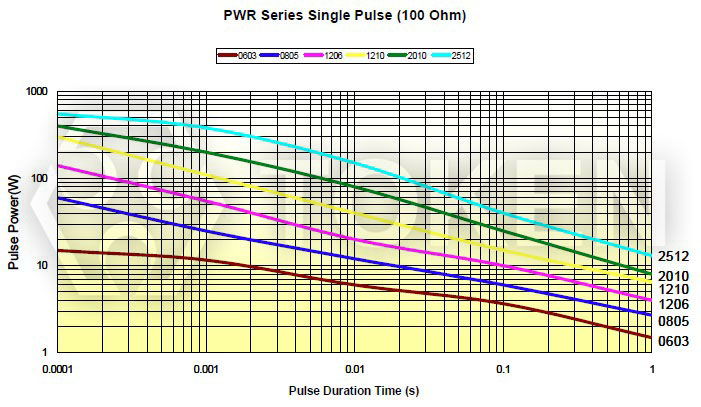
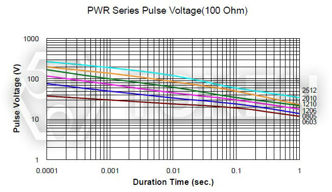
Pulse withstanding capacity of Pulse Withstanding Chip Resistor (PWR)
|
||
| Note: | The single impulse graph is the result of 50 impulses of rectangular shape applied at one-minute intervals. The power applied was subject to the restrictions of the maximum permissible impulse voltage graph shown. The limit of acceptance was a shift in resistance of less than 1% from the initial value. |
|
Continuous Pulse of Pulse Withstanding Chip Resistor (PWR)
|
|||
| Note: | The continuous load graph was obtained by applying repetitive rectangular pulses where the pulse period was adjusted so that the average power dissipated in the resistor was equal to its rated power at 70°C. Again the limit of acceptance was a shift in resistance of less than 1% from the initial value. | ||

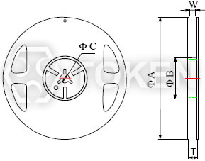
Packaging Quantity & Reel Specifications (Unit: mm) (PWR)
|
||||||||||
| Codes | Packaging Quantity (KPcs) | Tape Width | Reel Diameter | ΦA (mm) | ΦB (mm) | ΦC (mm) | W (mm) | T (mm) | ||
| PWR03 PWR05 PWR06 PWR13 |
Paper
|
5K | 8mm | 7 inch | 178.5±1.5 | 60+1/-0 | 13.0±0.2 | 9.0±0.5 | 12.5±0.5 | |
| 10K | 8mm | 10 inch | 254±1 | 100±0.5 | 13.0±0.2 | 9.0±0.5 | 13.5±0.5 | |||
| 20K | 8mm | 13 inch | 330±1 | 100±0.5 | 13.0±0.2 | 9.0±0.5 | 13.5±0.5 | |||
| PWR10 PWR12 |
Embossed
|
4K | 12mm | 7 inch | 178.5±1.5 | 60+1/-0 | 13.0±0.5 | 13.0±0.5 | 15.5±0.5 | |
| 8K | 12mm | 10 inch | 250±1 | 62±0.5 | 13.0±0.2 | 12.5±0.5 | 16.5±0.5 | |||
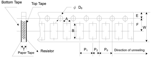
Paper Tape Specifications (Unit: mm) (PWR)
|
|||||||||||
| Codes | A (mm) | B (mm) | W (mm) | E (mm) | F (mm) | P0 (mm) | P1 (mm) | P2 (mm) | ΦD0 (mm) | T (mm) | |
| PWR03 | 1.10±0.10 | 1.90±0.1 | 8.0±0.2 | 1.75±0.1 | 3.50±0.05 | 4.00±0.10 | 4.00±0.05 | 2.00±0.05 | 1.50+0.1,-0 | 0.70±0.1 | |
| PWR05 | 1.60±0.10 | 2.40±0.2 | 8.0±0.2 | 1.75±0.1 | 3.50±0.05 | 4.00±0.10 | 4.00±0.05 | 2.00±0.05 | 1.50+0.1,-0 | 0.85±0.1 | |
| PWR06 | 1.90±0.10 | 3.50±0.2 | 8.0±0.2 | 1.75±0.1 | 3.50±0.05 | 4.00±0.10 | 4.00±0.05 | 2.00±0.05 | 1.50+0.1,-0 | 0.85±0.1 | |
| PWR13 | 2.90±0.10 | 3.50±0.2 | 8.0±0.2 | 1.75±0.1 | 3.50±0.05 | 4.00±0.10 | 4.00±0.05 | 2.00±0.05 | 1.50+0.1,-0 | 0.85±0.1 | |
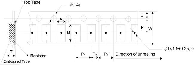
Emboss Plastic Tape Specifications (Unit: mm) (PWR)
|
|||||||||||
| Codes | A (mm) | B (mm) | W (mm) | E (mm) | F (mm) | P0 (mm) | P1 (mm) | P2 (mm) | ΦD0 (mm) | T (mm) | |
| PWR10 | 2.8±0.10 | 5.5±0.10 | 12.0±0.3 | 1.75±0.1 | 5.5±0.05 | 4.00±0.10 | 4.00±0.1 | 2.00±0.05 | 1.50+0.1, -0 | 1.2+0 | |
| PWR12 | 3.5±0.10 | 6.7±0.10 | 12.0±0.3 | 1.75±0.1 | 5.5±0.05 | 4.00±0.10 | 4.00±0.1 | 2.00±0.05 | 1.50+0.1, -0 | 1.2+0 | |
Pulse Withstanding Chip Resistors (PWR) Application & Soldering Notes
Today's electronic devices are becoming smaller and smaller. The requirement, in particular, for pulse withstand capability is growing due to the need to protect sensitive modern electronic systems.
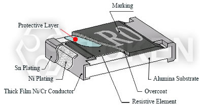
To meet this demand Token Electronics have designed a Pulse Withstanding Chip Resistor (PWR Series). The enhanced performance of the chips is made possible by the precise use of the best resistance inks and a closely controlled production process.
Application Notes:
- Applications vary from line protection for telecommunications to surge withstanding resistors for use in circuit breakers. Details of a typical telecomm and power supply application are given below.
- Telephone lines can be subjected to a large range of voltage disturbances, many of which can damage switching equipment. This has led to the need for circuit protection against both high voltage transients, usually of short duration caused by lighting strikes and overloads of longer duration, due to direct connection to mains power lines.
- These two faults are separated into primary and secondary protection.
- Primary protection handles the high voltage transients, and is usually located within the exchange.
- Secondary protection is usually built into the equipment to be protected, and deals with both current and voltage limiting.
- Voltage limiting prevents damage to the equipment and shock hazards, and current limiting prevents damage to wiring.
- To determine the suitability of a (PWR) series chip resistors for your application refer to the pulse withstanding data as given lighting surge performance using both 1.2/50μs and 10/700μs pulse shapes.
Soldering Notes:
- Electrical connection to a ceramic substrate or to a printed circuit board can be made by
reflow or wave soldering of wrap-around terminations. - Wrap-around terminations provide good leach properties and ensure reliable contact.
- Due to the robust construction, the (PWR) can be immersed in the solder bath for 30 seconds at 260°C.
- This enables the resistor to be mounted on one side of a printed circuit board and wire-leaded components applied on the other side.
- (PWR) resistors themselves can operate at a maximum temperature of 155°C.
- For soldered resistors, the joint temperature should not exceed 110°C.
- This condition is met when the stated power levels at 70°C and recommended pad and trace areas are used.
- Allowance should be made if smaller areas of copper are used.
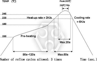
Recommend Soldering Condition (PWR)
|
Order Codes (PWR)
| PWR | 05 | D | TR | C1 | W | 10R0 | ||||||||||||||||||||||||||||||||||||||||||||||||||||||||||||||||||||||||||||||
 |
|
|
|
|
|
|
|
|||||||||||||||||||||||||||||||||||||||||||||||||||||||||||||||||||||||||||||
|
|
|
|
|
|
|
|
|||||||||||||||||||||||||||||||||||||||||||||||||||||||||||||||||||||||||||||
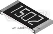
0805~2512 4 digits marking for Example Marking
| Resistance | 100Ω | 2.2KΩ | 10KΩ | 49.9KΩ | 100KΩ | 1MΩ |
| Marking | 1000 | 2201 | 1002 | 4992 | 1003 | 1004 |
0603: 3 digits nominal Table E24 Marking
| E24 code | 10 | 11 | 12 | 13 | 15 | 16 | 18 | 20 | 22 | 24 | 27 | 30 | 33 | 36 | 39 | 43 | 47 | 51 | 56 | 62 | 68 | 75 | 82 | 91 |
- Example: 101=100Ω 102=1KΩ (1st and 2nd are E24 code and 3rd code is multiplier)
- Resistance tolerance 1% for 0603: 3 digits marking in E96 (E96 series except E24 series)
- Digits marking for Example: 13C=13K3Ω; 68B=4K99Ω; 68X=49.9Ω
Marking Table E96 Marking
| code | 02 | 03 | 04 | 06 | 07 | 08 | 09 | 10 | 11 | 13 | 14 | 15 | 16 | 17 | 19 | 20 | 21 | 22 | 23 | 24 | 25 | 26 | 27 |
| E96 | 102 | 103 | 107 | 113 | 115 | 118 | 121 | 124 | 127 | 133 | 137 | 140 | 143 | 147 | 154 | 158 | 162 | 165 | 169 | 174 | 178 | 182 | 187 |
| code | 28 | 29 | 31 | 32 | 33 | 34 | 35 | 36 | 37 | 38 | 39 | 40 | 41 | 42 | 43 | 44 | 45 | 46 | 47 | 48 | 49 | 50 | 51 |
| E96 | 191 | 196 | 205 | 210 | 215 | 221 | 226 | 232 | 237 | 243 | 249 | 255 | 261 | 267 | 274 | 280 | 287 | 294 | 301 | 309 | 316 | 324 | 332 |
| code | 52 | 53 | 54 | 55 | 56 | 57 | 58 | 59 | 60 | 61 | 62 | 63 | 64 | 65 | 66 | 67 | 68 | 69 | 70 | 71 | 72 | 73 | 74 |
| E96 | 340 | 348 | 357 | 365 | 374 | 383 | 392 | 402 | 412 | 422 | 432 | 442 | 453 | 464 | 475 | 487 | 499 | 511 | 523 | 536 | 549 | 562 | 576 |
| code | 75 | 76 | 77 | 78 | 79 | 80 | 81 | 82 | 83 | 84 | 86 | 87 | 88 | 89 | 90 | 91 | 92 | 93 | 94 | 95 | 96 | ||
| E96 | 590 | 604 | 619 | 634 | 649 | 665 | 681 | 698 | 715 | 732 | 768 | 787 | 806 | 825 | 845 | 866 | 887 | 909 | 931 | 953 | 976 |
Multiplier E96 Marking
| Code | A | B | C | D | E | F | X | Y |
| Multiplier | 100 | 101 | 102 | 103 | 104 | 105 | 10-1 | 10-2 |